
Through-Holes PCB: Everything You Need to Know
Get Your PCB Quote!
Table of Contents

As printed circuit boards (PCBs) get smaller, they use fewer and fewer through-hole components. It is increasingly difficult to justify allocating precious space to relatively large plated through holes and corresponding pads. Instead, surface-mount components must be used whenever possible. With the increasing popularity of surface mount technology, the majority of plated through holes on most modern PCB designs are ultimately through holes.
The primary purpose of any PCB through-hole is to provide a conductive path to carry an electrical signal from one circuit layer to another through the plated hole walls. However, there are different types of vias, and there are no the same options for the final appearance of the via on the PCB surface. Although all through-holes have the same function, each type of visa needs to be accurately defined in the documentation so that assembly goes smoothly and the PCBA operates reliably.
Through-Hole Structures – Straight-Through, Blind, Buried:
The first type of vias is a
Via
This is a hole that goes all the way from the top layer to the bottom layer. It is open at both ends to allow the plating fluid to flow through and coat the hole walls to make it conductive. Visas are not drilled as long as the manufacturer’s rules for minimum diameter, maximum aspect ratio (board thickness divided by hole diameter), and contiguity (minimum allowed distance from the edge of one via to the nearest adjacent via) are followed.
Next are mechanically drilled
Blind vias
A blind via is drilled from the top or bottom layer but stops at a point before traveling the full distance through the PCB. Mechanically drilled blind vias can connect an outer layer to an adjacent layer and in some cases to another layer below, but careful planning is required to ensure good results. Unlike through holes, blind vias are open only at one end, so the plating solution cannot flow through the hole. This complicates the plating process.
The most common complication is that air bubbles can become trapped at the bottom of the hole, resulting in void areas with no copper coverage. To eliminate voids, it is best to use larger holes, smaller aspect ratios, and more vigorous plating agitation, which will allow air bubbles to escape and expose the hole walls, allowing for reliable plating. Understand the manufacturer’s design rules and apply them when you need to use such vias. Proper design coupled with good process control will result in high yields.
Next are mechanically drilled
Buried vias
These are used to connect internal layer structures only. Through holes are drilled from top to bottom of the stacked internal structure (such as L2-L7 of an 8-layer PCB) before being plated and filled in preparation for final lamination.
Sometimes blind vias connect only the inner layer pairs before lamination. In certain high-density applications, small outer layer features (such as BGA or QFP pads) can be connected to buried structures via laser microvias. The final “stacked” structure is equivalent to a through hole, but uses less outer layer space than a mechanically drilled via would.
Laser micro vias are the smallest type of visa, typically about 0.003″-0.004″ in diameter. The biggest advantage of micro vias is their ability to fit on very narrow pad areas, typically as a via-in pad within a tight pitch SMT or BGA package. After plating, the pad is planarized to its original smooth state, restoring the pad surface so it can be used for component welding.
The maximum aspect ratio of laser microvias is very small – typically about 1:1 – so for most applications, it is only practical to connect one layer to its adjacent layers through a very thin sheet of dielectric. In extremely dense designs, they can be stacked on top of each other in a sequential stack-up similar to that used for stacking buried vias.
First, the vias are laser drilled, plated, and planarized to form an interconnect from the outermost layer to the layer below it. Once these steps are complete, another layer is laminated to the outside of the stack. After lamination, the new layer goes through another cycle of blinding via drilling and plating. This connects the outermost layer to the adjacent layer. This process can usually be repeated 3-4 times if necessary.
Methods for Covering or Filling Vias
It is often desirable to perform additional treatments on vias later in the production sequence to improve thermal performance or assembly yield. These may include epoxy hole filling, an auxiliary welding mask, or some combination of the two.
These additional process steps are generally designed to eliminate assembly problems such as welding shorting between component pads and via pads or welding migrating down the barrel of a via that has been drilled into a component welding area. These problems lead to expensive troubleshooting and rework. Fortunately, most problems can be eliminated by specifying the proper treatment.
A tented via has a non-conductive welding mask covering the pads on either end of the hole. Tenting was popular when the dry film welding mask was at its best, as the 0.004-inch thickness of the dry film allowed it to very reliably tent even larger holes without the chance of cracking. Today, however, dry film masks are no longer used because their height causes difficulties with modern surface mount welding. The decline and disappearance of dry film have made this old tenting impractical, as modern LPI welding masks are only about one-tenth as thick and do not form a true tent.
A tented via has a welding mask over most of the pad, but the welding mask is only a few thousandths of an inch away from the hole. For medium-density PCBs, this is a good compromise between full insertion and doing nothing at all. A welding mask effectively increases the distance between the via and nearby solderable pad, reducing the likelihood of welding bridging from the pad to the via. Because the hole is open, there is no concern about contaminants being trapped or air pockets forming in the barrel of the hole. When preparing the Gerber file, size the welding mask opening for the affected hole to be the hole diameter + 0.004. Example: 0.010 via, 0.014 Gerber mask opening.
PCB via processing
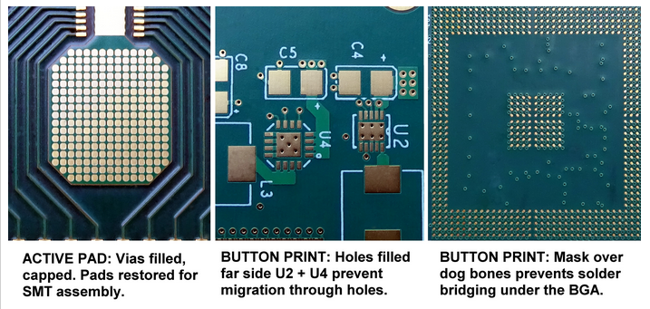
Button prints and plugged vias are variations of filled holes. They prevent welding from flowing (migrating) so that the correct amount of welding remains on the pad during assembly. The recommended material for these processes is non-conductive epoxy hole fill. Limit the maximum diameter of the via to 0.020 inches to allow the epoxy to effectively fill the hole. For these types, provide your Gerber files with a welding mask without the visa.
Active pads not only plug the hole but also the board. Often referred to as “via-in-pad,” “covered-in-pad,” or VIPPO, they are necessary if the pad originally used to drill the via will later be used to weld a surface-mount component. The via draws heat to the other side of the board to dissipate the heat, which is also useful for cooling hot-running components.
In an active pad process, a plug is used, pulled through by a vacuum, flattened, and over-plated. The resulting surface is usually indistinguishable from other SMT pads that have never been drilled. For this type, provide your Gerber files with welding mask openings without the associated via.
How to Define Visa Requirements
To avoid PCB issues, it is important to clearly state via requirements for TYPE and TREATMENT in your manufacturing documentation so you get the results you expect. In all cases, provide a separate file for each set of vias used in your design.
For TYPE, provide the following information to your manufacturer:
Type of visa (through, blind, or buried)
Via diameter (we recommend between 0.008″ – 0.020″)
Tolerance (usually +/- 0.003″, although smaller or blocked vias may be + 000/hole diameter)
Layer pair to connect per drill file (if blind or buried).
Example: Drilling a 0.008″ blind from TOP layer 1 to GND layer, 0.008″ finished + 0.000″ / – 0.008″.
For treatment, provide the following information to the manufacturer:
Treat all _____ diameter vias with a welding mask and dip into pads, but do not fill holes, per Gerber file (name).
Plug vias (partial fill): Use button print or IPC Class 4 treatment with non-conductive epoxy for all _____ diameter holes.
Plug vias (100% fill): Use IPC Class 5 treatment with non-conductive epoxy for all _____ diameter holes.
Fill and cap all _____ diameter vias per IPC Type VII. Fill holes, level, and cover with non-conductive epoxy. Apply surface treatment on pads.
Strive for the best result
Shenzhen Pcbandassembly SMT: Any unclear place in the PCB manufacturing instruction document may delay the quotation, affect the bare PCB delivery, or complicate the assembly cycle. With the advent of higher density designs, clear requirements for via type and treatment have higher importance than in the past. Keep in mind that different contract manufacturers have different preferences, and no the same PCB manufacturers may not use all the same equipment and materials. This puts you at risk of providing only Gerber welding mask files without openings for vias, expecting one manufacturer to deliver the same board as another. Instead, clearly state everything through requirements, and check to make sure your data files meet those requirements. Taking the time to accurately describe your project will eliminate unpleasant surprises later.
Table of Contents

Get Your PCB Quote!


