
Rigid PCB Manufacturing
Rigid PCB Manufacturing, From Prototype to Production
In-house rigid PCB fabrication with direct factory service
Rigid printed circuit boards are built on solid substrate materials such as FR4, delivering dimensional stability, mechanical strength, and long-term reliability under mechanical and thermal stress.
- 1–64 layer rigid PCBs
- FR4, High-Tg and halogen-free materials
- Prototype, low-volume and mass production
Production-ready fabrication
Rigid PCBs Built for Stable, Repeatable Production
We provide end-to-end rigid PCB manufacturing using precision CNC drilling, multilayer lamination, and fine-line imaging systems. Our processes support single-sided, double-sided, and multilayer rigid boards.
Engineering support covers PCB design, substrate selection, interconnect reliability, lead-free solder readiness, impedance control, and requirements review before fabrication.
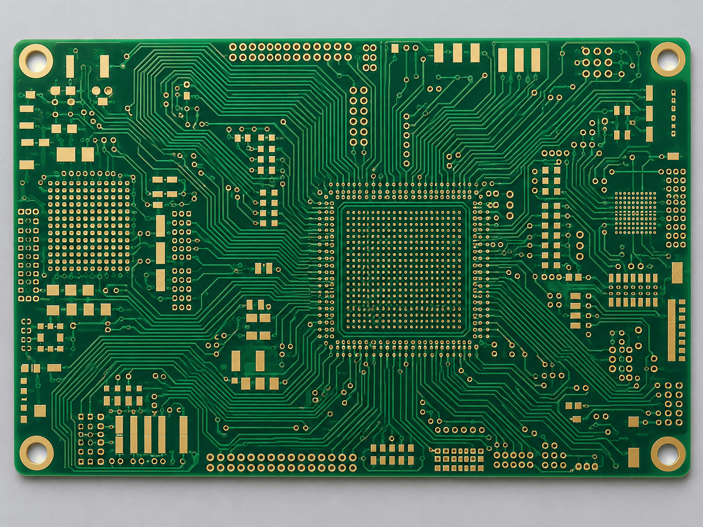
Scalable volume
Support for rapid prototypes, low-volume orders, and repeat production.
Material options
FR4, High-Tg FR4, halogen-free, CEM-3, and Rogers high-frequency materials.
Integrated service
PCB fabrication can be coordinated with component sourcing and PCB assembly.
Core capabilities
Our Rigid PCB Manufacturing Capabilities
From multilayer registration and fine-line imaging to heavy copper deposition and surface finishing, the service is designed to support production consistency across a wide range of rigid-board constructions.
Multilayer fabrication
1–64 layers using balanced stack-ups, HDI via-in-pad, staggered structures, or buried-core designs.
Fine-line imaging
Minimum line width / spacing of 1.8 mil with LDI imaging for dense routing and compact pad arrays.
Heavy copper
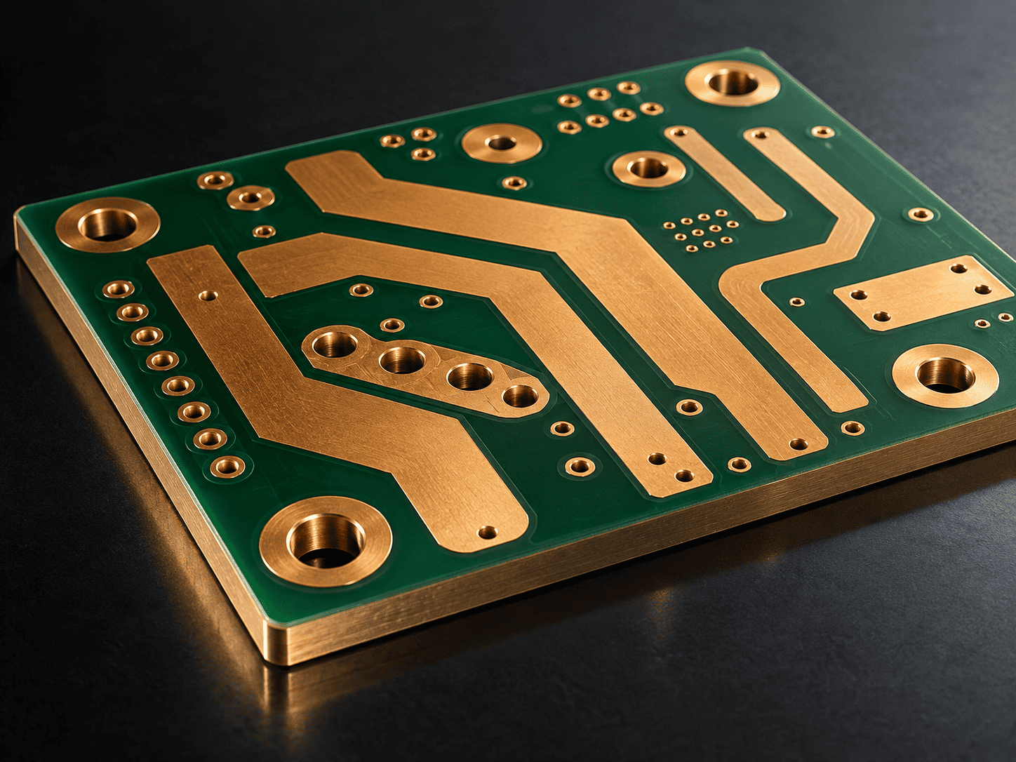
Copper weights from 0.33 to 28 oz per layer for high-current and thermal-performance applications.
Mechanical control
Board profiles, routing, V-score, tab routing, cut-outs, slots, chamfers, and production panelization.
High-current constructions
Heavy Copper With Controlled Plating and Stack-Up Review
Rigid boards can be manufactured with copper weights from 0.33 to 28 oz per layer for power conversion, current carrying, and thermal-performance requirements. Mixed copper weights and thick-copper geometry are reviewed against resin fill, spacing, etching, and finished-board thickness.
- 0.33–28 oz per layer
- Inner / outer weight combinations
- Cross-section verification
- Project-specific spacing review
| Specification | Details |
|---|---|
| Materials | FR4, High-Tg FR4, halogen-free material, CEM-3, Rogers HF material |
| Layer counts | 1–64 layers |
| Minimum finished PTH diameter | 0.08 mm |
| Finished copper thickness | Up to 1000 μm |
| Maximum board thickness / hole ratio | 40:1 |
| Finished board thickness | 0.1–12 mm |
| Minimum solder-mask bridge | 3 mil; minimum SMD pad space 8 mil |
| Minimum line / trace width | 1.8 mil |
| Surface finishes | Leaded HASL, lead-free HASL, ENIG, OSP, immersion tin, immersion silver, and others |
| Solder-mask colors | Green, black, blue, white, yellow, matte, and others |
| Other techniques | Gold fingers, peelable mask, blind / buried vias, characteristic impedance control |
| Warpage and twist | ≤0.5% |
| Flammability | 94V-0 |
Capability combinations depend on material, copper weight, stack-up, geometry, tolerances, and testing requirements. Final requirements are confirmed during quotation.
Board types
Rigid PCB Constructions We Support
Choose the board construction around routing density, thermal load, mechanical requirements, material system, and target production volume.
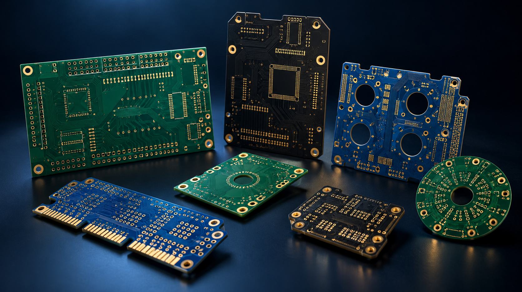
One manufacturing partner, multiple rigid-board platforms
Our current service page covers six rigid-board categories. Standard FR4 designs can be scaled from simple single-sided boards to dense multilayer builds, while High-Tg and metal-backed constructions address elevated thermal or mechanical demands.
Rigid-flex is included where rigid component sections need integrated flexible interconnects.
Single-Sided Rigid PCB
One copper layer on FR4 or CEM-1 for straightforward, cost-sensitive routing.
Double-Sided Rigid PCB
Top and bottom copper layers with plated connections for greater routing density.
Multilayer Rigid PCB
4–64 bonded layers with signal, power, and ground planes separated by dielectric spacing.
High-Tg Rigid PCB
High-Tg substrate systems such as S1000H and IT180 for repeated lead-free solder cycles.
Rigid-Flex PCB
Rigid cores and flexible layers combined where compact folding or integrated movement is required.
Metal-Backed Rigid PCB
Aluminum- or copper-backed constructions for LED, automotive, and power-conversion designs.
Materials & finishes
Build the Stack-Up Around the Application
A rigid PCB combines an insulating substrate, patterned copper, bonding prepreg, solder mask, and silkscreen into a fixed laminated stack. Material choice and surface finish affect temperature capability, solderability, contact life, signal behavior, and cost.
Discuss Your Stack-UpSubstrate
FR4, halogen-free, and High-Tg materials form the mechanically stable dielectric base. High-Tg options support lead-free soldering and sustained operation at elevated temperatures.
Copper layers
Patterned copper forms traces and power planes. Inner and outer copper weights can be selected separately for signal, current-carrying, and heat-transfer requirements.
Solder mask
LPI solder mask insulates copper, defines pad areas, and protects the board surface. Green, black, white, red, blue, yellow, and matte options are available.
Surface finish
ENIG, OSP, immersion silver, immersion tin, HASL, and lead-free HASL are selected around assembly, flatness, contact, storage, and RoHS requirements.
Silkscreen
Non-conductive epoxy legend supports component references, polarity markings, and assembly identification without interfering with exposed copper.

Quality control
Inspection Planned With the Build
Testing scope should match the board construction, density, impedance requirements, and end-use acceptance criteria. Confirm required reports and standards with the manufacturing enquiry.
AOI
Checks etched features and visible pattern defects against production data.
Electrical test
Flying-probe or fixture testing checks continuity and isolation.
Impedance test
Controlled traces can be verified to the agreed target and tolerance.
Microsection
Cross-section analysis supports plating and interconnect verification where specified.
How it works
From Manufacturing Data to Finished Boards
A clear handoff reduces quotation delays and helps the engineering team confirm construction, tolerances, testing, and delivery requirements before production.
Submit Your Files
Send Gerber or ODB++ data, drill files, fabrication drawing, quantity, and target delivery date.
Engineering Review
Review materials, stack-up, copper, hole structure, impedance, surface finish, and acceptance criteria.
Confirm the Quote
Agree the manufacturing specification, price, lead time, and any tooling or test requirements.
Fabricate & Inspect
Boards proceed through manufacturing, the agreed inspection plan, final packing, and shipment.
Application fit
When Should You Use a Rigid PCB?
Rigid PCBs are a strong fit when the assembly needs mechanical stability, precise component alignment, dense placement, or predictable high-volume production.
Stable product geometry
Supports fixed housings, heavier components, and assemblies that must remain flat and dimensionally stable.
Cost-focused production
Standardized FR4 processes, repeatable tooling, and established material systems support scalable manufacturing.
Shorter lead-time targets
Stocked rigid-board materials and repeatable fabrication steps help simplify production planning.
High component density
Stable substrates support dense BGA and QFN placement with controlled pad geometry and board thickness.
Added for faster quoting
What to Prepare for Your PCB Quote
Providing these items together gives the manufacturing team enough context to assess the build, highlight missing constraints, and return a more useful quotation.
Manufacturing data
Gerber or ODB++, NC drill files, and board outline.
Fabrication drawing
Finished dimensions, tolerances, holes, slots, cut-outs, and special notes.
Stack-up requirements
Layer count, finished thickness, copper weights, material, and impedance targets.
Commercial requirements
Prototype and production quantities, target delivery date, testing, reports, and shipping destination.
Frequently asked questions
Rigid PCB Manufacturing FAQs
What is the difference between rigid PCB and rigid-flex PCB?
Rigid PCBs are made entirely on solid FR4 or High-Tg laminate and remain flat after fabrication. Rigid-flex boards combine rigid sections with flexible polyimide layers, allowing defined areas to bend or fold during installation.
What is the minimum rigid PCB thickness?
The current service page lists finished rigid-board thicknesses down to 0.1 mm. Final feasibility depends on the material, panel format, copper distribution, layer count, tolerances, and handling requirements.
Can rigid PCBs use mixed copper weights?
Yes. The service supports differential copper thicknesses across inner and outer layers, allowing signal layers and power layers to use different copper weights. Mixed-weight builds require stack-up and resin-flow review.
How do you control dimensional stability on large rigid PCBs?
Dimensional control is managed through balanced stack-ups, controlled press cycles, core and prepreg matching, copper distribution review, profiling control, and warpage measurement after thermal processing.
What affects the final PCB quotation?
Layer count, board dimensions, quantity, material, copper weight, hole structure, line width and spacing, surface finish, impedance control, tolerances, testing, and delivery requirements all influence the quote.
Request a quote
Ready to Manufacture Your Standard PCB?
Send your board files, stack-up requirements, quantity, testing needs, and target delivery date. Our team will review the manufacturing details with your enquiry.
- 01Gerber / ODB++ and drill files
- 02Fabrication drawing and stack-up
- 03Quantity, testing, and delivery needs
