
HDI PCB Manufacturing Service
HDI PCB Manufacturing for Microvia, Blind & Buried Via Designs
HDI PCB
Custom HDI PCB fabrication from prototype to production, supporting laser microvias, via-in-pad, sequential lamination, controlled impedance, and high-density multilayer stackups.
HDI PCB Services You Can Rely On
HDI PCBs, or High-Density Interconnect printed circuit boards, are designed with fine lines, blind and buried vias, and dense via-in-pad routing to increase connection pad density while reducing size and weight. Our HDI products are manufactured to meet tight PCB layout requirements, utilizing high-quality materials and refined design techniques.
| Capability | Service Range |
| HDI Structures | 1+N+1, 2+N+2, 3+N+3, stacked and staggered microvias |
| Via Technology | Laser microvia, blind via, buried via, via-in-pad, copper-filled via |
| Materials | FR4, High-Tg FR4, Rogers hybrid, low-loss materials by request |
| Surface Finish | ENIG, OSP, immersion silver/tin, lead-free HASL where suitable |
| Inspection | AOI, X-ray, E-test, microsection, impedance test |
These boards reduce layer count, enable fine pitch BGA layout, and maintain stable signal paths in dense digital systems. We support HDI PCB prototyping and production from 1 to 10,000+ units with fast lead times and full turnkey PCB assembly.
Our HDI PCB Manufacturer Capabilities
Why Choose OrienwPCB as Your HDI PCB Manufacturer?
OrinewPCB provides end-to-end control across PCB fabrication, material selection, and inspection processes to support complex designs with tighter tolerances, fewer layers, and better signal performance. Each board is built to meet the demands of high-speed, high-density interconnect applications.
What is HDI PCB?
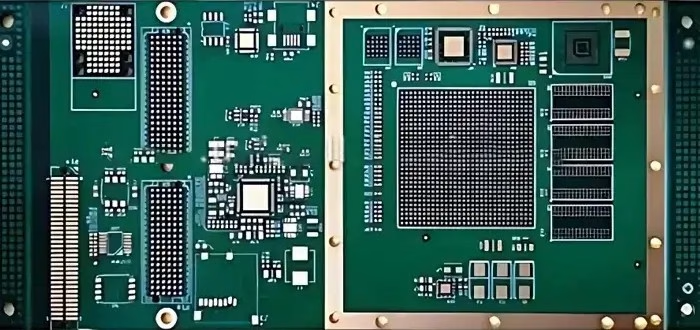
A high-density interconnect PCB is a multilayer board with a higher wiring density per unit area than standard designs, achieved through the use of microvias, blind and buried vias, and 2 to 3 mil trace widths. HDI PCBs have finer spaces and lines, minor vias and capture pads and higher connection pad density. It is helpful in enhancing electrical performance and reduction in weight and size of the equipment. HDI PCB is the better option for high-layer count and costly laminated boards.
HDI technology originated in the early 2000s with single microvia layers and has progressed to multi-build-up configurations with stacked, copper-filled vias used in mobile, automotive, and aerospace designs.
HDI PCB vs. Standard PCB
| Aspect | Standard PCB | HDI PCB |
| Component Density | Typically <100 pins/in², limited by mechanical via size and trace spacing | ≥120 pins/in² supported through microvias, fine lines, and via-in-pad routing |
| Drilling Method | Mechanical drills only; min hole diameter ≈ 6 mil | Laser drilling for microvias down to 4 mil with tighter positional tolerances |
| Via Structures | Through-hole only, with long z-axis path | Blind vias, buried vias, stacked and filled microvias with controlled depth |
| Trace/Space Capability | Commonly 5 to 6 mil trace/space | 2.5 mil / 2.5 mil or finer with LDI registration accuracy to ±12 μm |
| Layer Count | 4 to 16 layers typically required for complex nets | Often 6 to 10 layers with optimized routing due to high interconnect density |
| Stackup Flexibility | Symmetrical cores with limited sequential build-up options | 1+n+1, 2+n+2, 3+n+3 with multi-cycle lamination process and custom dielectric setups |
| Routing Efficiency | Long signal paths and via stubs increase EMI and reduce bandwidth | Shorter routing with minimal via stubs improves signal integrity and reduces EMI |
| Impedance Control | Basic control using microstrip/stripline; wide tolerances (±10 to 15 Ω) | Modeled to ±5 Ω using hybrid PCB laminate sets and calibrated TDR measurements |
| Support for Fine Pitch | Not compatible with BGA pitches under 0.5 mm | Fully supports fine pitch (≤0.3 mm) CSPs and dense I/O arrays |
| Board Size and Thickness | Larger footprints and thicker profiles due to higher layers of a PCB | Reduced form factor with fewer layers and thinner dielectric stacks |
| EMI Performance | Susceptible to loop-area EMI from long traces and through-vias | Improved EMI control via short transitions and tightly stacked interconnect boards |
| Fabrication Cost | Lower for low-density applications with basic features | Higher per unit, but offset by reduced layer count, smaller board size, and routing gains |
| Application Suitability | General consumer, hobbyist, low-frequency circuits | Advanced PCB designs in telecom, automotive, aerospace, and portable electronics |
Types of HDI PCB Structures
HDI designs are classified from Type I to Type VI based on the number and placement of microvia layers. Type I includes a single-layer microvia with no buried vias. Type II introduces buried vias beneath one build-up layer. Type III and higher include stacked microvias, filled and plated, across multiple layers. Type IV to VI use coreless substrates or every-layer interconnect (ELIC) for full vertical routing flexibility.
| Structure Type | Via Configuration | Supported Scale |
| 1+N+1 | Single-layer build-up with blind vias | Prototype, small to large-scale production |
| 2+N+2 (Staggered) | Dual-layer build-up with staggered blind and buried vias | Prototype, small to large-scale production |
| 2+N+2 (Stacked) | Dual-layer build-up with stacked blind and buried vias | Prototype, small to large-scale production |
| 3+N+3 | Triple-layer build-up with stacked vias across HDI layers | Prototype, small to medium-scale production |
Note: “N” represents the number of standard layers between the outer HDI layers. All constructions are fabricated using sequential lamination and resin-filled microvias for electrical and thermal stability.
