Causes and Improvement Methods of PCB Deformation and Damage
Get Your PCB Quote!

Table of Contents
- U proizvodnoj liniji za automatsku površinsku montažu, ravnost štampane ploče (PCB) je ključna.
- Da bi se analizirali uzroci deformacije PCB-a, potrebno je uzeti u obzir više faktora kao što su materijal, struktura, distribucija uzoraka i proces obrade.
- Kako poboljšati protumjere za sprječavanje savijanja ploče i savijanja ploče iza ploče?
In an automatic surface mount production line, the flatness of the printed circuit board (PCB) is crucial.
If the PCB surface is uneven, it will cause component positioning deviations, which will affect the correct insertion or connection of the components to the holes and surface pads of the circuit board. Not only can this misalignment potentially damage the automatic cassette loader, but it can also cause the soldered circuit board components to bend and damage the alignment of the component feet. In addition, uneven circuit boards are difficult to install into sockets inside the chassis or machine, causing a lot of inconvenience to assembly plants.
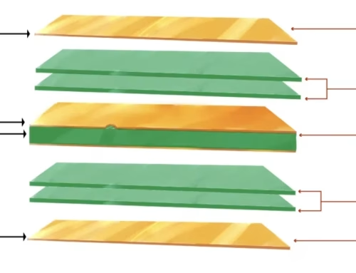
Currently, surface mount technology is developing towards high precision, high speed, and intelligence, which puts forward more stringent requirements for the flatness of PCB boards. PCB boards are composed of copper foil, resin, and glass cloth. These materials have different physical and chemical properties, resulting in residual thermal stress and deformation during the lamination process. In addition, the high temperature, mechanical cutting, and wet processing processes that PCBs undergo during processing will also have a significant impact on the flatness of the board. Due to the complex and diverse causes of PCB board deformation, how to reduce or eliminate deformation has become one of the complex challenges faced by PCB manufacturing companies, which involves differences in material properties and processing techniques.
To analyze the causes of PCB deformation, multiple factors such as material, structure, pattern distribution, and processing process need to be considered.
This article aims to analyze and explain the various causes of deformation and how to improve them. In circuit boards, uneven distribution of copper foil over an area of spread can cause board bending and deformation. Usually, the circuit board design includes a large area of copper foil as a ground layer, and sometimes the Vcc layer is also designed as a large area of copper foil. When the copper foil is not evenly distributed in these large areas, it will cause inconsistent heating and cooling rates. In this case, the circuit board will experience thermal expansion and contraction, and if the expansion does not occur evenly, it will cause stress differences and deformation in different parts. If the temperature of the circuit board reaches the limit of its glass transition temperature (Tg value), the board will begin to soften and then produce permanent deformation.
Current printed circuit board (PCB) designs generally use multi-layer structures, in which there are connection points between rib pins and each layer (through a hole). These connection points are mainly divided into three types: through holes, blind holes, and buried holes. The location of the connection point has a limiting effect on the expansion and contraction of the board, which may indirectly cause the board to bend or warp. In the normal reflow oven operation, the board is usually driven on both sides by chains to be processed in a preheating manner. This defect becomes noticeable when the board is too heavy or too large during support, as a depression may appear in the middle.
How do you improve countermeasures to prevent board bending and board warping behind the board?
Temperature is the main factor that causes plate stress, and its changes have a significant impact on the stress state of the plate. By lowering the temperature of the reflow furnace or adjusting the heating and cooling rates of the board in the furnace, the bending and warping of the board can be effectively reduced. However, this move may be accompanied by other adverse effects. High Tg sheets refer to sheets with a higher glass transition temperature, which marks the critical point where the material transitions from the glassy to the rubbery state. A board with a lower Tg value will soften faster after entering the reflow oven, but it will also take longer to reach a rubbery state, resulting in increased deformation of the board. By using a plate with a higher Tg value, its ability to withstand stress and deformation can be enhanced, but accordingly, the material cost will also increase.
In electronic product manufacturing, to achieve thinner and lighter designs, the thickness of circuit boards has been reduced to 1.0 mm, 0.8 mm, or even 0.6 mm. Therefore, maintaining the flatness of the circuit board in the reflow oven is challenging. In the absence of professional advice on thin circuit boards, it is recommended to use a thickness of at least 1.6 mm to significantly reduce the risk of bending deformation. In addition, reducing the size of the circuit board and the number of splices are also effective strategies to reduce distortion. Since the circuit board mainly relies on chains to move forward in the reflow oven, its weight may cause dents and deformations. Therefore, the long side of the circuit board should be kept parallel to the reflow oven chain as much as possible to reduce deformation caused by the weight of the circuit board itself. Reducing the number of components is also based on this consideration. It is claimed that the smallest dent deformation can be achieved using a furnace shape that is as similar as possible to a narrow vertical furnace.

Get Quote Free