Get Your PCB Quote!

Table of Contents
Advanced processing technology is essential to the manufacturing of electronic goods. SMT is an innovative electronic processing technology which has dramatically altered how electronics products are manufactured. Surface Mount Technology, also referred to as SMT, has had an enormous effect on product creation processes. This article will introduce SMT and its characteristics, application areas, process flow and future development trends in detail.
1. SMT Overview
Surface Mount Technology (SMT) is a production and assembly method used to directly attach electronic components onto printed circuit board (PCB). This allows for automated production of more assembly required to create a board. Surface mount devices (SMD/SMC) are electrical components mounted this way. As we all know, traditional electronic component assembly technologies use plug-in technology, where pins of components are inserted through holes on a printed circuit board and secured using solder. SMT does not entail inserting components through holes but directly solders them onto the board via reflow soldering. SMT is highly regarded for its cost-effectiveness and efficiency.
First created by IBM in the 1960s as surface mount technology, SMT became widely adopted for minicomputer manufacturing after replacing through-hole technology with SMT components; reaching 10% market penetration until 1986. By 1990, surface mount devices or SMD could be found in most high-tech printed circuit board assembly (PCBA).
SMT components are smaller than through-hole parts, enabling the production of stylish electronics suitable for today. SMT technology has found its way into many types of electronic devices on the market – from phones and laptops to toys and kitchen appliances.
2. SMT Features
SMT technology’s history can be traced to the 1960s when a US-based company created a technology for assembly called “coordinate placement” which allows electronic components to be accurately placed according to predetermined angles and positions. This technology was first used in the aviation and military fields and then gradually moved into the civilian electronic field. The advantages of SMT are mainly in the following aspects:
Miniaturization
SMT allows components be mounted directly onto the PCB surface, without drilling holes. This can significantly reduce the size and weight of components, making the product more compact and lightweight, and achieving miniaturized design of electronic products.
High Density
Since the pin design of SMT is smaller, the spacing between components can be denser, and more components can be integrated in a limited space, thereby improving the integration of the circuit.
Lightweight
SMT uses chip components that are only a few tenths, or even a handful of hundredths, of the size of plug-in components. This allows for greater assembly density, and lighter electronic products.
Wide Adaptability
SMT technology can be applied to various components, from traditional passive devices like resistors and capacitors, to micro-packaged chip components such as integrated circuits.
High Reliability and High Shock Resistance
Solder paste is used to bond components onto PCB boards. This improves mechanical strength and reliability. SMT allows chip components to be positioned closer together due to their light weight and small size. This improves the reliability and performance.
SMT also allows for better electrical connections, a reduction in resistance and crosstalk during signal transmission. SMT uses a tin-lead soldering alloy that is shock resistant. It is a high-frequency material that reduces electromagnetic interference and has good characteristics.
Low Production Costs and High Efficiency
SMT automation equipment is able to place and weld at high speeds, compared with the traditional plug-in method. This greatly improves production efficiency, and reduces manufacturing costs. SMT components are compact, saving energy and raw materials. Automated equipment can simplify the production process, and save time and manpower costs.
In many ways, SMT is beneficial for PCB assembly, electronic product manufacturing and PCB production. SMT has its own disadvantages:
Poor Maintainability
Chip components are easily broken and fragile in SMT. It is very difficult to fix a problem once it occurs because these components are welded to the circuit board. To replace these components during maintenance, special tools and equipment are needed. The welding technology is also quite high.
High Initial Cost
The miniaturization of solder joints and their variety complicates the detection and process. In addition, the complexity and cost of the technology require high levels of training and education.
SMT is a great way to design and produce electronic circuits, particularly complex ones. The entire electronics industry benefits from this higher level of automation. SMT remains a viable technology even though new developments are possible.
3. Application Fields of SMT
SMT technology has multiple applications, from communication equipment and consumer electronics to automotive electronics. SMT is important in these fields.
1) Consumer Electronics Industry:
√ Smartphones and tablets: SMT technology is widely used in the assembly of smartphone and tablet motherboards, camera modules, battery management systems and other components. SMT enables mobile phones to have a smaller body, higher performance and longer battery life.
√ Audio and video equipment: For example, numerous components on the internal circuit boards of televisions, stereos, DVD players, etc. are assembled using SMT patch technology.
√ Other consumer electronic products: For example, refrigerators, electronic doors, etc., these products usually require high-density electronic assembly. SMT patch technology can provide fast and accurate assembly solutions to meet consumers’ requirements for product performance.
2) Computer and Communication Industry:
√ Computer motherboards and servers: The CPU, memory, chips and other key components on the computer motherboard and the various boards inside the server all rely on SMT patch technology for assembly.
√ Network equipment: For example, communication equipment such as routers, switches, wireless AP, etc., the components of their internal circuit boards are mostly assembled using SMT patch methods.
√ Satellite communication and navigation systems: The communication and navigation modules on satellites require high-reliability and high-precision electronic components’ assembly, and SMT patch technology is an important means to achieve this goal.
3) Automotive Electronics:
√ Engine Control Unit (ECU): The ECU controls the engine. It integrates numerous electronic components, which are tightly assembled on the circuit board through SMT patch technology. SMT can achieve efficient integration and reliability of vehicle electronic systems, improve driving safety and driving experience.
√ In-car entertainment system: Including car audio, navigation system, display screen, etc., the components on its circuit board also widely use SMT patch technology.
√ Safety systems: For instance, anti-lock braking systems and body stabilization systems such as ABS/ESP require high precision SMT patch technology for reliable connection of electronic components.
√ Vehicle control system: As one of the core applications within automotive electronics, vehicle control systems serve to manage sensor signals and regulate actuators according to predefined programs. In these control systems, SMT technology has been widely used. Sensors are essential elements of automotive electronic control systems, and many sensors utilize Surface Mount Technology for miniaturization and high precision production.
4) Industrial Control Field:
√ PLC (Programmable Logic Controller): The core control device in the field of industrial automation, which integrates numerous electronic components on its internal circuit board, and these components are assembled with high density through SMT patch technology.
√ Sensors and actuators: Industrial automation often utilizes sensors, actuators and circuit boards equipped with SMT patches for ease of assembly and repair.
5) Medical Electronics Field:
√ Medical monitor: A device that monitors the vital signs of a patient. The components on its internal circuit board are precisely assembled through SMT patch technology.
√ Medical imaging equipment: Such as X-ray machines, CT scanners, etc., their internal electronic control systems are also inseparable from SMT patch technology.
√ Other medical equipment: Such as medical monitors, blood glucose meters, etc., also widely use SMT patch processing technology.
6) New Energy and Aerospace Fields:
√ New energy industry: For example, solar inverters, electric energy meters, battery management systems, electric drive systems, and on-board chargers in new energy vehicles all require SMT processing technology.
√ Aerospace field: The military and aerospace fields have high requirements for the quality and reliability of electronic equipment, and SMT patch technology can also meet these requirements, providing high-density and high-reliability electronic assembly solutions, generally used in radar systems, satellite communication equipment, missile control systems, etc.
7) Other Fields:
√ LED lamps and displays: Circuit boards and control modules in LED lighting products, the components on which are mostly assembled using SMT patch technology to achieve efficient and energy-saving lighting effects.
√ Art and creative industries: Electronic products in these industries often have unique appearance and functional design. Using SMT patch processing technology, electronic components can be embedded in products to achieve more diverse creative effects.
SMT technology’s widespread use has led to the miniaturization of electronic devices, their multi-functionality, and the production of mass products with low defect rates.
4. SMT Production Process
Manual assembly of SMD components can be time-consuming and precise work. To increase productivity and increase efficiency, most SMT production today utilizes automated assembly machines for efficient production. This is especially true in mass production. SMT equipment includes: placement machines, reflow-soldering, plugs, wave-crest ovens and test packaging equipment.
The SMT production process involves multiple key links, which require strict control and management from material preparation to cleaning and packaging.
1) Preparation of Materials
Material preparation is the first step of SMT production. The first step in the SMT production process is material preparation. This includes purchasing and inspecting materials like PCB, electronic components such as pads, solder, etc. The pads are flat copper or silver pads with tin-lead, gold, or tin-lead plating. They support the pins on components like transistors and chip.
2) PCB Pretreatment
Before SMT production, PCB needs to be pretreated. Generally, this step entails three processes for PCB production: cleaning, drying and inspection. Cleaning removes dirt and oxides on its surface in order to ensure quality welding; drying ensures moisture does not interfere with its effect; while inspection screens out any defective pieces that might enter subsequent production stages.
3) Solder Paste Printing
The printing of solder paste is an important part of SMT production. The equipment needed are: fully automatic printer, three-dimensional solder paste detection equipment (SPI). First, the corresponding steel mesh needs to be made according to the PCB pad design. Then, the steel mesh is placed on the PCB, and the solder paste is evenly printed on the pad by the printer. In this step, the amount and uniformity of the solder paste have a crucial impact on the subsequent welding quality.
Solder paste is used to connect pads on SMD and PCB. Each pad must have the correct amount of paste applied. If the solder does not melt in the reflow, then the connection cannot be made.
Note:
√ The printing process is not complete without selecting the correct solder paste. Solder paste selection should depend on the specific requirements for soldering, such as type and material of components soldered to PCB boards, etc. To allow time for its natural defrosting process to occur, store solder paste in the freezer 12-24 hours before use and take it out 12-24 hours before you need to use it.
√ The size of the steel mesh is also critical to the printing process. The size of the steel mesh machine is generally 550-650 mm. The machine cannot print if the steel mesh is not large enough.
√ SPI: Solder paste detector, detect whether the solder paste printing is good or not, and do not allow the occurrence of undesirable phenomena such as insufficient tin, tin leakage, excessive tin, tin connection, and offset.
√ During the printing process, ensure the accuracy and uniformity of the printing, ensure that the solder paste has enough rolling volume on the steel mesh, and replenish the solder paste in time. For the defective printing products, they must be carefully cleaned, and the steel mesh must be wiped in time.
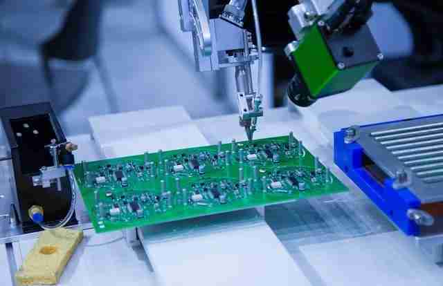
4) Component Placement
Component placement is the core link in the SMT production process, and the main equipment used is a multifunctional placement machine. The placement machine must be programmed and debugged first. It should then be programmed with the coordinates for the location of patch components based on the BOM sample patch location map supplied by the client.
Mounting components on PCB is done using pick and place machines. Remove each component from the packaging using a vacuum cleaner or gripper. Then, a placement machine will place it at the designated location. The PCB boards move on a conveyor belt. Electronic components are then placed by machines that are fast and precise. Some of these machines can place up to 80,000 components per hour.
The accuracy and stability of the chip mounter directly affect the quality of component placement. In this step, the position of the mounted components needs to be corrected to ensure that they are accurately placed in the predetermined position. If there is a wrong placement, it may be expensive and time-consuming rework.
Note:
√ Precision and debugging of the patch machine: The precision and stability of the patch machine directly affect the accuracy of component placement, and regular calibration and maintenance are required. According to the size and shape of the components, adjust the parameters of the patch machine to achieve the best placement effect.
√ Patch order: first paste small and low components, then paste large and high components. For small components, only one patch position is required, while large components need to occupy 2~3 patch positions, which will also affect the efficiency of the patch factory. According to the compiled program, the position of the components is arranged, and a material report (including material model, requirements, published position, etc.) is formed to form a sample seal for record.
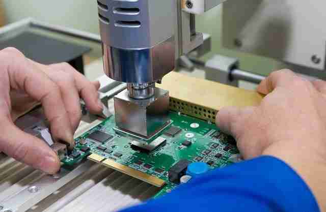
5) Reflow Soldering
Reflow soldering must be done after the components have been mounted. The equipment required is a reflow-oven. Heating the PCB enables solder paste to melt, allowing components to be securely attached. Reflow soldering requires temperature and time management as well as careful attention paid to monitoring defects such as cold soldering or short-circuiting during soldering processes.
Temperature and timing are crucial elements in the reflow process, and must be set according to the solder properties and PCB material properties. Keep an eye on the temperature curve in the reflow oven to ensure consistency and stability during soldering.
6) Quality Inspection and Repair
The PCB must be checked for quality after soldering. This includes appearance inspection, electrical performance test, and X-ray inspection. Through these inspection methods, problems that may occur during the soldering process can be discovered and handled in a timely manner. Errors discovered during SMT inspection will require repairs or re-soldering in order to preserve product quality. Magnifying glasses, automatic optical inspection (AOI), flying probe testers and X-ray inspection are among the various methods of inspection available.
Automatic Optical Inspection (AOI)
Use automatic optical online inspection to detect whether the soldered boards have any defects: wrong parts, missing parts, reverse, multiple parts, reverse side, offset, less tin, more tin, empty solder, tin beads, side stand, pin warping, and foreign matter. AOI can detect defects with high accuracy and speed, thereby improving product quality and production efficiency.
Visual Inspection (Manual Inspection)
The key items to be checked in manual inspection are:
√ Whether the version of the PCBA is the changed version;
√ Whether the customer requires the use of alternative materials or components of specified manufacturers and brands;
√ Whether the directions of components with directions such as IC, diodes, transistors, aluminum capacitors, switches, etc. are correct;
√ Check for welding defects, such as false parts, false welds, open circuits, short circuits, etc.
X-RAY Detection
For components of multi-layer PCB or BGA packaging types, X-ray inspection can penetrate the surface layer and detect the internal welding conditions. X-ray inspection can find welding defects hidden inside and further improve product quality. X-RAY equipment inspection is widely used in BGA inspection, LED, SMT, semiconductor, electronic connector module inspection, packaged components, aluminum die castings, molded plastic parts, ceramic products, electrical and mechanical parts, automation components, agriculture (seed inspection), 3D printing analysis and other industries. In the processing plant, for example, QFN packaging, the bottom of the pad cannot be seen and can only be viewed through X-RAY equipment.
7) Cleaning and Packaging
The last step is cleaning and packaging. Cleaning is done to remove any residues or flux from the PCB surface to increase the reliability and stability. The PCB boards are packaged after cleaning to avoid damage or contamination while transporting and storing.
The most common packaging method is anti-static bags or anti-static cotton in separate packaging. Put it in the blister tray and spread it out for packaging, mainly for PCBA boards that are sensitive to needles and have fragile patch components.
5. Development Trends of SMT
Future development trends in SMT will be mainly based on the following:
Smaller and More Sophisticated
The requirements for SMT continue to increase with the development of electronic technology. SMT is expected to become smaller and more sophisticated in the future. The result will be a lower volume of components, and a greater assembly density.
Smarter and More Efficient
Automation equipment and artificial-intelligence technology will be employed to increase production speed and efficiency.
More Environmentally Friendly and More Sustainable
SMT technology’s future will become more eco-friendly and energy efficient through the incorporation of materials that protect the environment as well as energy saving technologies.
6. Summary
The SMT technology has become a major milestone in modern electronics manufacturing. Its revolutionary development has had a huge impact on circuit board assembly and electronic product manufacturing. By realizing surface mounting and high-density integration of electronic components, SMT technology has achieved size reduction, performance improvement and production efficiency improvement. In the future, with the further development of science and technology, SMT technology will continue to innovate and optimize, providing more possibilities and broad development space for electronic products.

Get Quote Free