A Complete Guide to PCB Assembly and Manufacturing: Process & Benefit
Get Your PCB Quote!

Table of Contents
Table of Contents
Printed circuit boards define the states of contemporary electronics. From smartphones to devices used in medicine, they form the foundation of the interplay between electrical connections and functionality. Understanding the assembly and manufacturing process goes a long way to allow informed decisions concerning quality and efficiency.
Understanding PCB Assembly
PCB assembly can be said to include the placing and soldering of electronic components onto the bare circuit board. This stage is crucial in converting that simple board into a working unit that is the power supply for various electronic devices.
Types of PCB Assembly
Various techniques are employed for assembling circuit boards, each of them conferring certain advantages with respect to their ultimate applications.
Surface Mount Technology (SMT)
A surface mount PCB provides a compact and highly efficient solution for upcoming electronics, ensuring excellent performance and reliability. SMT is the most widely used technique due to its ease and compactness in design.
Through-Hole Technology (THST)
THT refers to inserting the leads of components through holes that were drilled through the board and soldered on the other side. This is primarily suited for components that need good mechanical support.
Mixed Technology
Some boards require combined SMT circuit board and THT methods for optimum performance. This hybrid practice is most often found in advanced electronic products.
The PCB Manufacturing Process
A PCB is manufactured in a series of steps ensuring reliability and functionality. Below are the important phases:
1. Design & Prototyping
The first step is to establish a circuit design through a dedicated software design package. Engineers define connections, placement of components, and signal paths. Upon approvals of the design, construction of a prototype is done for testing purposes.
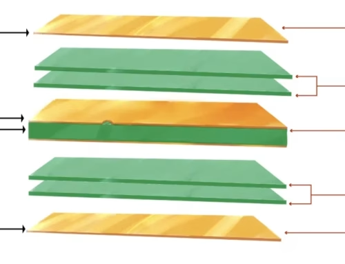
2. Material Consideration
Material exert impact onto the durability and performance. Common materials include:
• FR4 – This is a fiberglass-reinforced epoxy laminate used for general purposes.
• Metal Core – For LED applications because they provide superior thermal properties.
• Flexible Substrates – Devices that are used in low-profile and bendable applications.
3. Printing and Etching
Photolithography, in turn, provides what is essentially inkjet printing, a method for applying the circuit pattern to the board. The subsequent etching removes unwanted copper and retains the desired traces.
4. Drilling and Plating
The drilled holes are used for the placement of components and electrical connections, and these holes are then plated to ensure conductivity between the circuit board layers.
5. Solder Masking and Silkscreen Application
The first solder mask to be applied, which serves to protect the copper traces from oxidation and solder bridges, is then followed by the silkscreen layer for labeling, marking, and identifying components.
6. Component Placement and Soldering
In this stage, the components are placed using an automatic pick-and-place machine. Different methods of soldering are then employed:
• For soldering surface – mounted components, reflow soldering is the method of choice. The board is painted with solder paste, which afterward enters the reflow oven, where all components are soldered down as solder paste melts. This is the chosen method as it proves accurate and works for compact designs.
• Wave soldering is used for through – hole components. The assembly is passed over a wave of molten solder, thus providing a strong electrical connection. This is particularly effective for larger components that require mechanical stability.
Both soldering techniques are crucial factors in providing a means to ensure the assembled board’s durability and reliability.
7. Inspection and Testing
To maintain quality, testing on assembled boards was done:
• High-level quality and functionality of assembled circuit boards guarantee thorough inspection and testing routes. The above-mentioned inspection is immediately followed by Automated Optical Inspection (AOI).
• On more complex assemblies, internal solder joints are verified using X-ray inspection, specifically for components containing grid array (BGA) where other optical methods become impossible to apply.
• Finally, functional testing is done in simulated operating conditions close to the real one. The board is powered and electrically tested to ensure that all components perform as desired.
8. Final Cleaning and Packaging
The boards are cleaned after testing to remove flux residues and other contaminants. Thereafter, they are carefully packaged for delivery or integration into devices.
Benefits of Quality PCB Assembly
A good circuit board creates an endless list of advantages:
1. Performance and Reliability
Adequately assembled, its board further reduces electrical faults in operation by maintaining steadiness, thus preventing failures.
2. Compact and Efficient Designs
Advanced assembly females miniaturize high-performance electronics while optimizing the utilization of space.
3. Cost-Effective Process
Application of efficient techniques in manufacturing reduces waste of materials at assembly error levels, thus lowering the overall production cost.
4. Suitable for Mass Production
Automated assembly lines permit high-volume production without compromising quality, making it an industry standard in high-demand sectors.
5. Customization and Versatility
PCBs can be customized to parameters specific to a design; therefore, they can be used across various applications.
Factors Influencing the Selection of PCB Manufacturer
Picking your choice of manufacturer would help guarantee high-quality production and the success on the road ahead. Keeping in mind the considerations mentioned below:
• Experience & Expertise – A well-timed provider guarantees the expertise on complex designs.
• Certifications & Standards – Compliance with the industrial standard by the PCB manufacturer ensures safety and reliability.
• Advanced Technology – The modern workshop reaches higher levels of precision and efficiency.
• Customer Support – Earnest help and technical support renders the process of raising issues easier.
What Lies Ahead for PCB Assembly
The rapidly changing electronic environment continues to experience major trends defining the future of circuit board assembly:
• Miniaturization: Everything is shrinking; new designs for PCBs must accommodate that.
• Flexible and Wearable Electronics: The industry is benefitting from these developments with exploitation of flexible circuits.
• Artificial Intelligence & Automation: AI-powered manufacturing is said to hold tight to precision and quality control.
• Eco-Friendly Resins: Eco-sustainable production is the growing trend.
Wrapping Up
Knowledge of the PCB assembly and manufacturing processes leads to worthwhile decisions in quality and performance. Technology, in all its glory, continues to push circuit boards into state-of-the-art innovation across different industries. Investing in a robust manufacturing process will grant electronics usability, efficiency, and affordability.

Get Quote Free