Everything you need to know about the PCB assembly Process
Each step of the process-from the design validation stage to the packing stage-has an important role to ensure that the final PCB board will work reliably.
Get Your PCB Quote!
Table of Contents
")
It is important, in a modern electronic environment, to have the functionality and performance highly dependent on the integration of each component onto the board. The process that begins bare and becomes an operational system has been long and arduous. Being aware of every detail of PCB and assembly processes could be helpful in proposing improved product quality, reliability, and life span.
The process, in any case, does require careful planning, tight control, and very advanced technology. Each phase, from design verification all through to the final inspection, is strictly controlled according to set standards. This manual will therefore show each stage of assembling a high-performance electronics board.
1. Design Verification and File Preparation
Before any assembly starts, Design Validation takes place. This phase has engineers reviewing the design files to make sure they conform to the intended application. Files may include the schematic layout, bill of materials, and Gerber files. They are blueprints that direct the entire manufacturing and assembly process.
Any issues related to component placement, spacing, or thermal reliefs are solved. Solving these issues allows for avoiding expenses in rework and delays down the track. File preparation is critical to aligning all subsequent processes, especially when producing a printed circuit board PCBA for high-reliability use.
2. Sourcing Quality Components
Once the design is finalized, sourcing components begins. All parts should conform exactly to what is stipulated in the bill of materials, be it resistors, capacitors, ICs, or connectors. Using parts of good quality that are certified is vital to ensure a strong electrical performance and a long period of service.
Project assemblers consider the availability of parts and alternative options, if necessary. Suppliers are rated for stability, certification, and history. These reputable suppliers are the ones used so that every batch of components satisfies the toughest quality criteria.
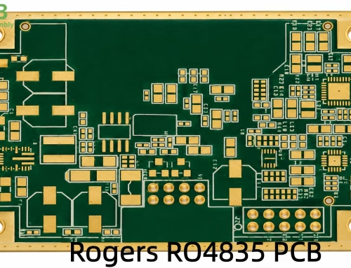
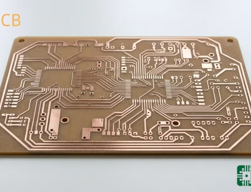
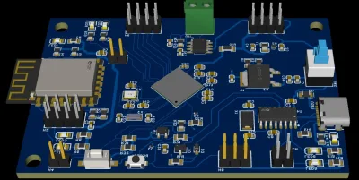
3. Preparing the Bare Board
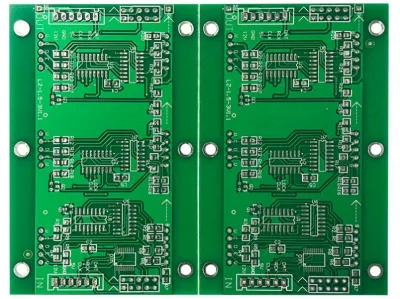
The assemble PCBs process starts with mounting boards. They are typically made from fibreglass reinforced epoxy laminate and copper layered; such boards go through an inspection for any defect, including misalignments in traces, holes, and delamination.
Surface finish application occurs at this point as well, serving to protect the exposed copper and ensuring solderability. The choice of a correct finish should be based on the application’s needs, shelf life considerations, and cost constraints.
4. Stencil Design and Solder Paste Application
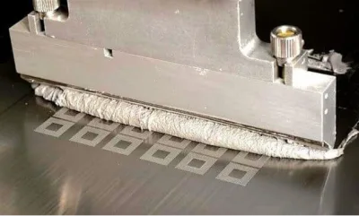
Solder paste printing is next. A stainless steel stencil is created that works off the pad layout from the PCB files. A stencil helps apply solder paste exactly where it’s needed on the board.
The solder paste is an amalgam of powdered solder and flux. It temporarily holds components in place and then forms a strong mechanical and electrical bond with the joint upon heating. It is important to have proper alignment and controlled application of the paste to prevent bridging or weak joints.
-
Stencil Precision & Area Ratio: To achieve optimal solder release, particularly for micro-components like 0201 or 01005, we utilize laser-cut, electro-polished stencils. The design adheres to the “Area Ratio” principle (typically > 0.66) to ensure consistent paste transfer and prevent insufficient solder joints.
-
3D SPI Inspection: Every board undergoes 3D Solder Paste Inspection (SPI) immediately after printing. This system monitors the volume, height, and alignment of the paste in real-time, allowing us to intercept up to 70% of potential soldering defects before they reach the placement stage.
Automated machines control the deposition for uniform application on all boards. Each board is then inspected for paste volume and alignment before component placement goes ahead.
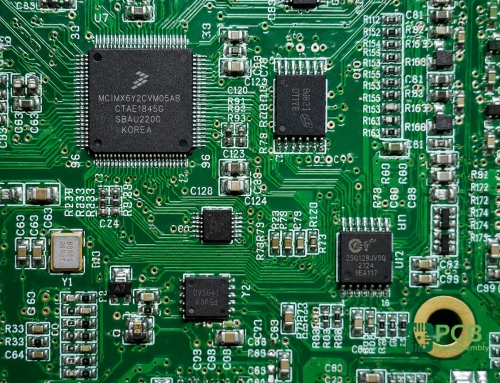
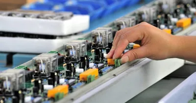
5. Automated Component Placement
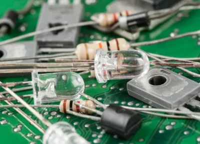
Surface-mounting of components onto the solder-pasted boards takes place at this stage. Being programmed via coordinate files from the design files, these machines pick parts from the reel or tray and place them with great accuracy.
Being able to place components by the thousands per hour with great precision, irregular or bigger components are usually hand-placed if necessary. Ensuring each component is in its correct location is vital for the next steps to succeed.
6. Reflow Process
After placement, the assembled board travels through a reflow oven. The soldering paste will then heat up, melt, and join firmly the components onto the pads. This oven is maintained under a temperature profile to avert thermal shock or warping.
Reflow soldering then solidifies the assembly, ensuring components are locked in place. Care is taken to apply appropriate heat such that the joints form properly without hazardous effects on sensitive parts. Afterwards, the board is electrically connected and mechanically stable upon cooling.
Thermal Profiling: The reflow process is governed by a precise thermal profile consisting of four critical stages:
-
Preheat Zone: Gradually raising the temperature to activate flux and prevent thermal shock.
-
Soak Zone: Ensuring thermal equilibrium across the entire PCB to minimize temperature gradients.
-
Reflow (Peak) Zone: Reaching temperatures above the alloy’s liquidus point (e.g., 217°C-220°C for SAC305) with a controlled Time Above Liquidus (TAL) to form a robust Intermetallic Compound (IMC) layer.
-
Cooling Zone: Managing the cooling rate to achieve a fine-grained solder structure for superior mechanical strength.
7. Functional Testing
Functional testing verifies if the printed circuit board PCBA is working correctly. Supply voltage is given to simulate operating conditions, and different parameters are measured-maybe voltage levels, signal integrity, timing, or logic states.
Test jigs or fixtures can be used to automate the whole process. This kind of testing is very important to identify faults which can’t be detected through inspection. They validate if a particular board works in real-world circumstances.
8. Final Cleaning and Conformal Coating
When a unit passes all the required tests, they are cleaned to remove flux residues, dust, or any contaminants. This step is important in reliability, especially for boards in harsher environments.
A conformal coating may then be applied, depending on its use. It is a thin layer that gives the unit protection from moisture, dust, and chemical exposure, going a long way in increasing the toughness. It is usually seen in automotive, aerospace, and industrial electronics.
9. Packaging and Delivery
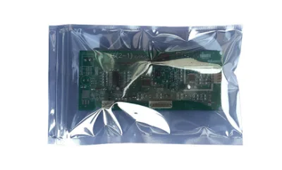
The concluding function in PCB assembly is to safely package it. Delicate boards must be sealed in an anti-static bag or custom-made trays to prevent physical or electrostatic damage. Some labels carry identification and tracking information. Packaging is also considered for moisture sensitivity, vibration protection, and safety during stacking. Correct environmental handling will ensure the product reaches its destination intact and ready for the final system integration.
10. Typical Issues with PCB Assembly
Though the concept is crystal clear, there are times when challenges arise. The component shortage, design errors, or soldering errors that cause delays and failures. That is why communication is essential among the parties, namely designers, engineers, and assemblers.
Moisture-sensitive components must be treated according to the procedure under consideration to ensure that cracking does not occur within the component. Also, the thermal profile must be optimised for each layout board, avoiding cold and overheated joints. Training, experience, and proper quality management must be in place to avoid rework or product recalls.
-
IPC Acceptance Standards: All assembly work is performed and inspected in strict accordance with IPC-A-610 Class 2 (General Electronic Products) or Class 3 (High-Performance/High-Reliability Electronics), ensuring international-grade quality and reliability.
-
MSD Management: We implement rigorous Moisture Sensitive Device (MSD) handling protocols. Components with high MSL (Moisture Sensitivity Levels) are stored in Humidity Indicator Card (HIC) monitored environments and pre-baked at 125°C when necessary to prevent “popcorning” effects during reflow.
11. Summary
Successfully assembled PCBs result from careful planning, qualified personnel, and precise equipment. Each step of the process-from the design validation stage to the packing stage-has an important role to ensure that the final board will work reliably.
Stepping through each process of assembly ensures the finer points are taken care of, no matter if it is consumer electronics, apparatus for use in medical treatment, or industrial controls. With proper methodology and equipment, manufacturers would be able to assure repeatability, surpass compliance requirements, and exceed customers’ expectations.
Table of Contents
Get Quote Free