PCB Vias Guide: Types, Standard Sizes & Design Tips
Discover everything about PCB vias, types, standard sizes, filled vias, via-in-pad, blind and buried vias. Essential 2025 guide for engineers and manufacturers.
Get Your PCB Quote!
Table of Contents
- 1. Que é exactamente unha vía para PCB?
- 2. 6 tipos esenciais de vías para PCB
- 3. Vía de PCB en Pad: Por que é importante
- 4. PCB con vías cheas: tipos e vantaxes
- 5. Tamaños estándar de vías para PCB
- 6. Por que as vías cegas e soterradas están a cambiar as regras do xogo
- 7. PCB de microvía en deseños avanzados
- 8. Vías térmicas: manter a electrónica fría
- 9. Desafíos de deseño con vías en PCB
- 10. Boas prácticas de deseño de vías de PCB
- 11. Aplicacións de diferentes vías de PCB
- 12. Consideracións de custo das vías de PCB
- 13. O futuro das vías para PCB
- 14. Antes de comezar a fabricar
- 15. Vías para PCB FAQs
Pop open a phone, a drone, or the brain of an EV and you won’t see the magic at first glance. What actually makes all that power fit into something so thin isn’t a single chip or a fancy connector, it’s a web of PCB vias quietly doing the heavy lifting.
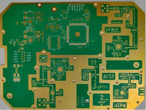
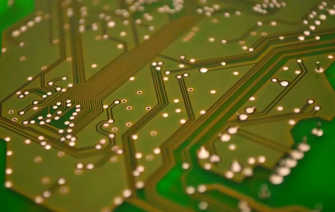
A printed circuit board via is basically a tiny tunnel through copper and fiberglass. Signals dive down one layer, pop up on another, and keep moving. Power follows. Heat, too. No vias, no multilayer boards. And without multilayer boards? No modern electronics as we know them.
Here’s what we’ll unpack in plain English: the main PCB via types (including blind and buried vias), when via-in-pad is a lifesaver for BGAs, how filled vias PCB processing keeps solder where it should be, and why PCB thermal vias keep hot parts honest. We’ll also talk standard PCB via sizes, what they cost you in the real world, and a handful of design habits that prevent painful respins.
Designing a board yourself or sourcing one through a partner like PCBandAssembly.com? Understanding vias and even through hole vias isn’t just trivia, it’s the difference between “works on my bench” and “works in production.”
1. What Exactly Is a PCB Via?
A circuit board via is a drilled and plated hole that connects copper traces from one layer to another in a printed circuit board via stack.
Every via has three parts:
- Pad– the copper surface where the via begins or ends.
- Barrel– the copper-plated hole that carries the signal vertically.
- Anti-pad– clearance on layers where the via should not connect.
When you hear about vias in PCB design, it’s really about managing complexity in multilayer circuits. Without vias, engineers would need massive boards or clumsy connectors.
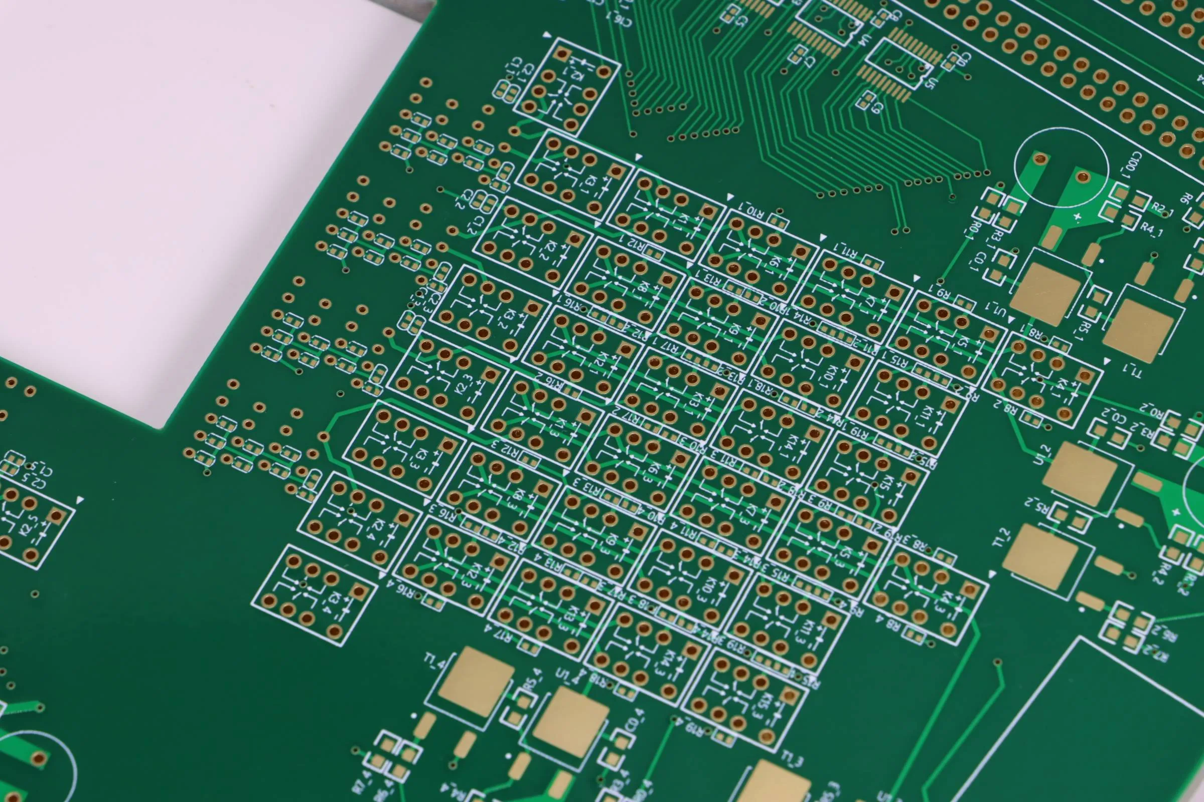
2. 6 Essential Types of PCB Vias
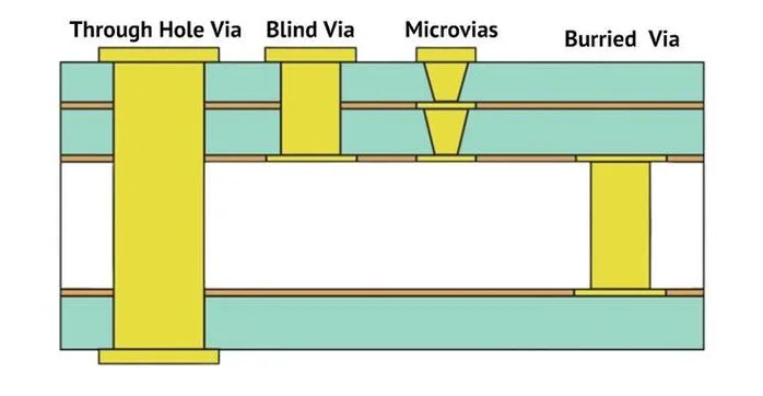
Not all vias are equal. Each type solves a different design challenge.
1) Through-Hole Via
The most common PCB via type is the through-hole via, drilled straight through from top to bottom. Cheap, simple, and reliable. But they take up routing space across all layers, which limits density.
2) Blind Via PCB
A blind via PCB only connects the outer layer to one or more inner layers. Think of it like an elevator that only goes halfway down. This frees up space and makes blind vias ideal for high-density interconnect (HDI) designs.
3) Buried Via PCB
A PCB buried via sits completely inside the board, connecting internal layers only. You can’t see it from the outside. Perfect for freeing up top and bottom layers for components.
4) Blind and Buried Vias Combination
In blind and buried vias designs, engineers mix both approaches. This combo is common in smartphones and aerospace electronics, where space is priceless.
5) Micro Via PCB
A micro via PCB uses laser drilling to create extremely small holes, often less than 0.1 mm. These are stacked or staggered across layers in HDI PCBs. They’re critical in advanced devices like 5G smartphones, wearables, and medical implants.
6) Thermal Vias PCB
A PCB thermal via doesn’t carry a signal. Instead, it transfers heat from hot components into copper planes. Without thermal vias, chips like CPUs or power regulators would overheat.
3. PCB Via in Pad: Why It Matters
If you’re working with BGAs or fine-pitch packages, you’ll hear about via-in-pad PCBs.
Instead of placing vias beside pads, engineers put the via directly inside the pad. Why? Because it saves space and reduces inductance in high-speed designs.
But there’s a catch: these vias must be filled and plated, otherwise, solder will flow into the via hole during assembly, leaving poor connections. That’s why via in pad PCB designs always use filled vias PCB techniques.
4. Filled Vias PCB: Types and Benefits
Filled vias PCB matter because they protect solder joints, improve heat flow, and keep high-speed signals stable. The fill you choose depends on what the board needs to do:
- Conductive fill (silver/copper epoxy).Use this when the via must carry heat or current as part of the circuit, under power devices, RF shields, or dense ground pads. You’ll see lower thermal resistance and a small drop in via impedance.
- Non-conductive fill (epoxy resin).Best for via-in-pad on fine-pitch BGAs. It blocks solder from wicking into the hole, keeps the joint flat for reliable assembly, and doesn’t change the net’s electrical behavior.
- Copper-filled vias.The premium route. These act like solid metal posts with excellent conductivity and heat spreading. They cost more but shine in power modules, high-reliability gear, and high-frequency PCBs that also run hot.
If you’re building RF front ends, compact power stages, or anything that mixes speed and heat, filled vias are often the difference between “works on the bench” and “works for years.”
5. Standard PCB Via Sizes
Choosing standard PCB via sizes without PCB via fill is a trade-off: smaller holes buy routing freedom and cleaner signal transitions, but they raise cost and manufacturing risk. Use the tightest geometry only where it actually improves density or signal integrity; keep the rest at a yield-friendly size.
| Via type | Typical drill | Typical finished hole | Common usage / pitch | Notes (cost & risk) |
| Through-hole via | 0.20–0.30 mm | 0.10–0.15 mm | General multilayer routing, power/ground stitching | Lowest cost, robust plating; consumes layer real estate across the stack |
| Micro via PCB (laser-drilled) | 0.075–0.10 mm | 0.050–0.075 mm | HDI breakouts; stacked/staggered layer jumps; 0.50/0.40 mm BGAs | Higher cost; tight process control; short stubs improve SI |
| Via-in-pad PCB (for BGAs) | 0.10–0.20 mm | 0.08–0.15 mm | Fine-pitch BGAs (≤0.80 mm, esp. 0.50/0.40 mm) | Requires fill + copper cap + planarization; best density and low inductance |
| Blind via | 0.15–0.25 mm | 0.10–0.18 mm | Surface to inner-layer escape; HDI | Moderate cost; helps free surface layers; watch aspect ratio |
| Buried via | 0.15–0.25 mm | 0.10–0.18 mm | Inner-to-inner connections; compact stacks | Higher cost; adds lamination steps; preserves outer-layer area |
| Thermal via arrays | 0.20–0.30 mm | 0.10–0.20 mm | Under hot devices (LEDs, VRMs) | Prioritize copper fill or dense arrays; focus on plane contact, not pitch alone |
As via diameter and aspect ratio shrink, price and process risk go up. If budget matters, deploy micro and via-in-pad only on nets and packages that need them, and keep the rest of the board on comfortable, high-yield sizes.
Need PCB Manufacturing or Assembly?
Get a free quote within 24 hours. We specialize in prototype-to-production PCB/PCBA for hardware teams worldwide.
6. Why Blind and Buried Vias Are Changing the Game
Blind vias connect an outer layer to inner layers; buried vias live entirely between inner layers. Together, they unlock HDI layouts by freeing the surface for components and short, direct traces. The practical wins:
- Smaller boards without sacrificing features.
- Cleaner escape routing from fine-pitch parts (shorter stubs, fewer layer jumps).
- Tighter component placement with fewer detours.
That’s why phones, laptops, wearables, and crowded IoT modules lean on blind and buried vias. In many designs, skipping them means a larger PCB, an extra layer count, or features that won’t fit at all.
7. Micro Via PCB in Advanced Designs
Laser-drilled micro vias are the HDI workhorse. Because they’re short and narrow, they introduce less parasitic inductance and capacitance, which helps high-speed signals behave. Three reasons engineers reach for micro vias:
- Signal integrity.Shorter vertical transitions reduce reflections and timing skew on high-frequency nets.
- Compact breakouts.You can escape dense BGA fields without burning entire layers on dog-bones.
- Stacking options.Stacked or staggered micro vias create controlled, layer-by-layer paths that keep routes short and predictable.
Yes, micro vias cost more than standard through-holes. But in aerospace, medical devices, automotive radar, and 5G handsets, the electrical headroom and space savings typically justify the spend.
8. Thermal Vias: Keeping Electronics Cool
A PCB thermal via works like a tiny heat chimney, pulling heat down from a hot pad and spreading it into the inner copper planes so your heatsink and airflow actually do their jobs. In practice, designers place thermal vias PCB arrays beneath exposed pads on LEDs, VRMs, and power ICs to cut junction temperatures and smooth out hot spots. Many small vias usually outperform a few large ones because you get more copper wall area and better contact with the plane; typical drills land around 0.20 – 0.30 mm on 0.5 – 1.0 mm pitch, tuned to your stackup and copper weight.
Tie each via into the largest continuous plane you have (ground, in most cases) and give that plane real copper mass, thin islands won’t spread heat. If the vias sit inside the pad, specify filled and capped to stop solder wicking and keep the pad perfectly flat for assembly; if they sit outside, tenting is fine and cheaper. Mirroring the array on the board’s opposite side, or adding a secondary plane, can drop temperatures further. Done well, thermal via networks deliver cooler operation, better reliability, and fewer performance throttles under load.(Learn more about[Tented vs. Untented Vias: Differences & How to Choose])
9. Design Challenges with Vias in PCB
Signal integrity gets touchy fast. A via that’s a few millimetres too long can act like a stub and reflect energy back into a high-speed trace. DDR, SerDes, and RF nets are the usual victims.
Costs creep in quietly. Start stacking blind via PCB and buried via PCB layers and your lamination steps multiply. The board stays the same size, but your quote doesn’t.
Reliability isn’t free. Push the aspect ratio and the copper plating can thin out in the barrel, leading to intermittent faults after thermal cycling. It may pass at the factory and fail in the field.
Thermal stress is real. Without enough copper around the barrel, or without nearby thermal vias, hot-cold cycles can micro-crack the via wall. You won’t see it until failure analysis.
If a via choice solves routing but forces three extra laminations or bumps aspect ratio past your fabricator’s comfort zone, it’s not a solution, it’s a future RMA.
10. PCB Via Design Best Practices
To design robust boards, follow these guidelines:
- Avoid vias in bend zonesin flex circuits.
- Keep aspect ratio below 10:1to ensure plating reliability.
- Use teardrop padsfor mechanical strength.
- Stitch vias togetherfor ground planes and thermal relief.
- Don’t overuse via-in-padunless necessary, it drives up costs.
- Simulate high-speed viasto check for impedance mismatches.
11. Applications of Different PCB Vias
1) General electronics: Standard through-hole vias handle everyday multilayer routing, stitching, and low-cost builds.
2) Mobile and wearables: Blind via PCB structures help escape fine-pitch BGAs without burning layers, keeping boards thin and batteries big.
3) Aerospace/medical: Buried via PCB connections keep outer layers clean for components and conformal coating while protecting inner-layer links.
4) 5G and high-speed compute: Micro via PCB stacks (staggered or stacked) shorten vertical transitions and tame parasitics in dense HDI.
5) Power and lighting: Arrays of thermal vias under regulators, MOSFETs, and LEDs move heat into planes so heatsinks actually work.
If you’re sourcing PCBs from China, the via strategy ties directly to cost and yield. A supplier like PCBandAssembly.com can tell you when a blind via saves a layer, and when it just adds a lamination cycle you don’t need.
About PCBAndAssembly
Time is money in your projects – and PCBAndAssembly gets it. PCBAndAssembly is a PCB assembly company that delivers fast, flawless results every time. Our comprehensive PCB assembly services include expert engineering support at every step, ensuring top quality in every board. As a leading PCB assembly manufacturer, we provide a one-stop solution that streamlines your supply chain. Partner with our advanced PCB prototype factory for quick turnarounds and superior results you can trust.
12. Cost Considerations of PCB Vias
Use this tiered view to compare process complexity, cost, and when each via type makes sense.
| Tier | Via type | Key processes | Relative cost | When to choose | Risks / notes |
| 1 | Through-hole | Mechanical drill, standard barrel plating | Lowest | General multilayer routing, stitching, power/ground | Consumes all layers; large stubs on fast nets if not back-drilled |
| 2 | Blind via PCB | Sequential lamination, controlled depth drill | Moderate | Escape routing from fine-pitch BGAs without adding full layers | Added lam cycles; watch aspect ratio and registration |
| 3 | Blind Buried vias PCB | Inner-layer drill + plate before outer lamination | Higher | Preserve both outer layers for dense parts or coating | More process steps; yield depends on stack precision |
| 4 | Micro via PCB | Laser drill, stack/stagger options, tight registration | Premium | HDI, 0.50/0.40 mm BGA breakouts, high-speed SI | Cost rises with stacking; strict fab capability needed |
| 5 | Via-in-pad (filled/capped) | Fill (non-/conductive), copper cap, planarize | Highest | Fine-pitch BGAs, low-inductance paths, compact thermal paths | Mandatory fill/cap; plan stencil and X-ray; expensive but high yield on dense designs |
Rule of thumb: Total Cost ≈ Base stackup + (Lamination steps × complexity) + (Special processes: laser, fill, cap, planarize).
Loop in your fabricator early, right-sizing vias can remove entire lamination cycles (and surprise line items).
13. The Future of PCB Vias
The role of vias is only growing. Trends in 2025 include:
- 5G and beyond.As line rates climb, micro via PCB transitions and back-drilled stubs will be standard practice, not “nice to have.”
- Electric vehicles.Tight control modules push HDI with blind and buried vias, packing more intelligence into smaller footprints without cooking the board.
- Data centers.PCB thermal vias scale from “good hygiene” to “design requirement,” moving heat away from hot spots so airflow and liquid cooling can do their job.
- Miniaturization everywhere.Via-in-pad becomes routine for sub-0.5 mm BGAs in AR/VR and IoT, where every fraction of a millimetre matters.
Smarter via strategies aren’t an optimization pass, they’re the architecture. The teams that get vias right ship smaller, faster, cooler products. The ones that don’t ship late.
14. Before you hit fabricate
PCB vias aren’t just holes; they’re the quiet architecture that makes modern hardware possible. From through-hole workhorses to blind, buried, and micro via PCB stacks, they let you pack more function into less space without sacrificing reliability. When density gets brutal, think sub-0.8 mm BGAs, via-in-pad earns its keep, provided you pair it with filled vias PCB processing so solder stays put and pads stay flat.
Heat is its own battle. Thermal vias move energy into planes so LEDs, VRMs, and processors run cooler and last longer. Even the “small” choices, your standard PCB via sizes, show up on the BOM: smaller holes can help signal integrity and routing, but they also raise cost and tighten manufacturing windows. And if you need maximum compactness, blind and buried vias unlock true HDI layouts for phones, wearables, and dense IoT gear.
Bottom line: choosing the right via strategy is half design, half manufacturing. If you want fewer surprises and better yield, partner with a factory that lives this every day, like PCBandAssembly.com
15. PCB Vias FAQs
1) What is a PCB via?
A printed circuit board via is a plated hole that connects copper layers in a PCB. It enables signals, power, or heat to move vertically through the stack.
2) What are the main PCB via types?
The common PCB via types are through-hole vias, blind via holess, buried vias, micro vias, and thermal vias. Each serves a unique role in design.
3) What is a blind via PCB?
A blind via PCB connects the outer layer to one or more internal layers. Unlike through-hole vias, blind vias don’t go all the way through.
4) What is a buried via PCB?
A PCB buried via connects inner layers only, invisible from the surface. Buried vias free up space on top and bottom layers.
5) What is via-in-pad?
PCB via in pad means placing vias directly under component pads, often for BGAs. These vias are usually filled to prevent solder defects.
6) Why are filled vias used?
Filled vias PCB designs use conductive or non-conductive fills to strengthen connections, improve heat transfer, and stop solder wicking.
7) What is a micro via PCB?
A micro via PCB uses laser drilling to create tiny vias. Common in HDI PCBs, micro vias improve density and high-frequency performance.
8) What is a PCB thermal via?
A PCB thermal via transfers heat away from hot components into copper planes, improving reliability and extending device lifespan.
9) How do PCB via sizes affect cost?
Smaller standard PCB via sizes (like micro vias) require advanced equipment and cost more. Through-hole vias are cheapest.
10) What’s the future of PCB vias?
Expect more reliance on micro via PCB and via-in-pad PCB designs for miniaturization, plus thermal vias for heat management in next-gen devices.

Get Quote Free