
Wearable PCB Assembly: Miniaturization & Flexibility
Wearable PCB assembly requires special optimization about size, reliability and flexibility based on the core of "human wearing," to meet the actual needs.
Get Your PCB Quote!
Table of Contents
In smartwatches, wireless earbuds, medical patches, smart glasses, and other wearable devices, PCB (printed circuit board) serves as the “hardware core carrier.” However, their assembly is not simply a scaled-down version of standard consumer electronics PCB. Constrained by the “human-worn scenario,” wearable PCB assembly must meet four critical requirements: “ultra-miniaturization, low-power adaptation, flexible compatibility (for some devices), and resistance to environmental interference.” Today, we start from the fundamentals to dissect the definition of wearable PCB assembly, its differences from traditional PCB assembly, core requirements, basic processes, and common issues—helping you build a systematic understanding.
1. What is Wearable PCB Assembly?
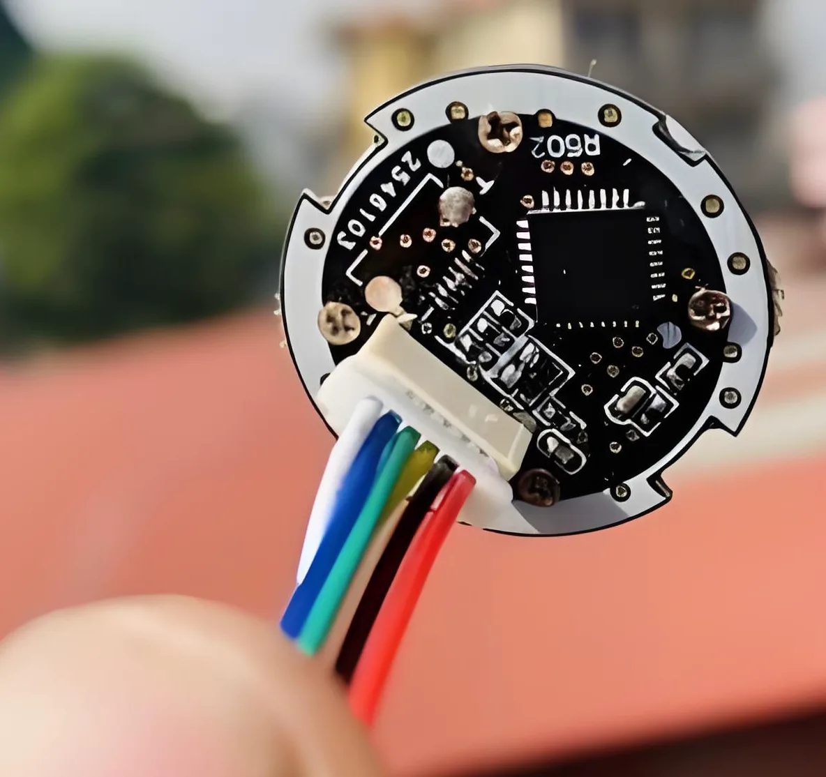
The core definition of wearable PCB assembly involves integrating chips, sensors, and passive components onto miniature PCB through specialized substrate selection, ultra-small component placement, precision soldering, and lightweight packaging. This process addresses the “miniaturization, low power consumption, and portability” requirements of wearable devices, ensuring stable operation in the “human-worn environment” (temperature 36-40°C, humidity 30%-70%, mild vibration). Its primary objectives are to meet four critical requirements: extreme miniaturization, low-power adaptation, high reliability, and flexible compatibility.
2. What are the Differences Between Wearable PCB Assembly and Traditional PCB Assembly?
Wearable PCB assembly demands higher standards in miniaturization, flexibility, environmental adaptability, and low power consumption, significantly increasing process complexity. Traditional PCB assembly, however, prioritize versatility and cost control. Specific comparisons are as follows:
1) Size and Component Density
Wearable PCBA: Typically measure less than 10cm² (e.g., smart earbud PCBA at 2cm × 3cm), with component densities reaching 100-200 components/cm²—2-3 times that of traditional PCBA. Utilize ultra-small package components like 01005 (0.4mm × 0.2mm) and 0201 (0.6mm × 0.3mm).
Traditional PCBA: Larger dimensions (e.g., mobile phone mainboard approx. 10cm × 8cm), lower component density, predominantly using conventional packages (e.g., 0402, 0603).
2) Substrate and Flexibility Requirements
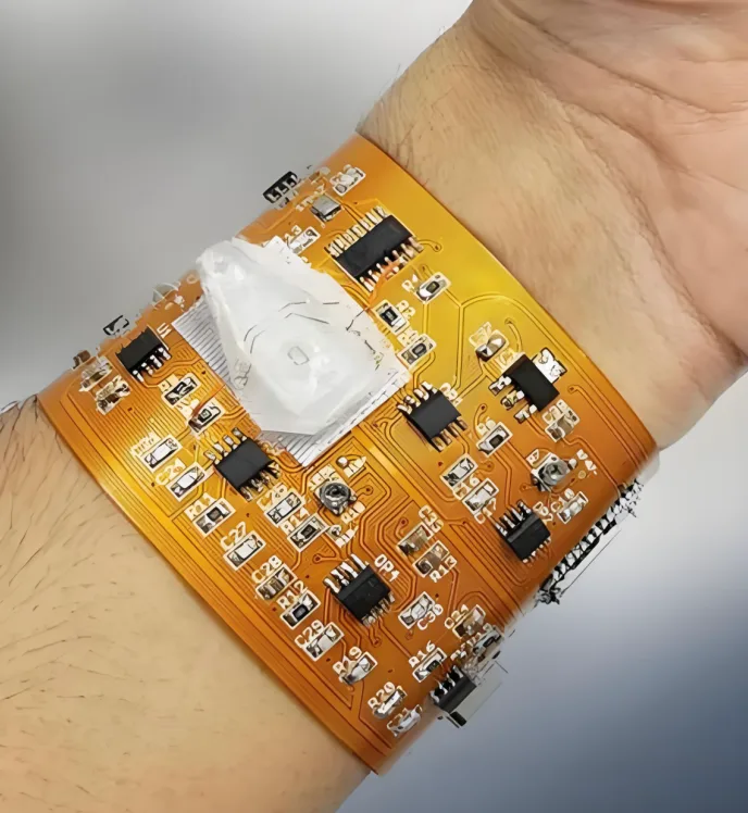
Wearable PCBA: Certain devices require flexible PCB (FPC), such as medical patches and smart bracelets, which must conform to the human body’s contours (bending radius ≥5mm). Additionally, the bending characteristics of flexible substrates must be considered to prevent substrate fracture during soldering. Common substrates are polyimide (PI) with thicknesses of 0.1-0.2mm.
Traditional PCBA: Primarily rigid substrates (e.g., FR-4) with thicknesses typically ≥0.8mm, requiring no consideration of bending properties.
3) Environmental Adaptability
Wearable PCBA: Must withstand human wear environments (temperature 36-40°C, humidity 30%-70%) and prolonged friction from prolonged wear. Requires resistance to sweat corrosion, waterproofing (e.g., IPX4 rating), and special protective assembly processes (e.g., waterproof coatings, anti-corrosion plating).
Traditional PCBA: Operate in relatively stable environments (e.g., room temperature and dry conditions) with no special protective requirements.
4) Process Challenges
Wearable PCBA:
Ultra-small Component Placement: Prone to misalignment and tombstone, requiring high-precision placement machines (positioning accuracy ±0.005mm) and electroformed stencils.
Flexible PCB Soldering: High temperatures easily cause substrate deformation, necessitating low-temperature reflow soldering (peak temperature 180-200°C).
Traditional PCBA: Mature process; standard reflow soldering (peak temperature 230-250°C) suffices.
5) Reliability Requirements
Wearable PCBA: Must operate continuously for 1-3 years, preventing cold solder joints and component detachment. e.g., Bluetooth chips in smart earbuds require high-reliability soldering.
Traditional PCBA: Relatively lower lifespan requirements, typically 3-5 years.
6) Low-Power Design
Wearable PCBA: Primarily battery-powered (50-500mAh capacity), requiring optimized routing to minimize signal loss. Often utilize low-power components (e.g., MCU sleep current ≤1μA).
Traditional PCBA: Lower power consumption requirements, typically powered by fixed power supplies.
3. What are the Fundamental Processes for Wearable PCB Assembly?
In fact, the fundamental processes for wearable PCB assembly are similar to traditional PCB assembly. However, to meet the specific requirements of wearable devices—such as ultra-miniaturization, low power consumption, and flexibility compatibility—each step requires optimization. Below are the core steps and key points:
1) Substrate Selection
Rigid PCB: Utilize ultra-thin FR-4 substrate (0.4-0.8mm thickness) with high-temperature resistance (Tg ≥ 150°C).
Flexible PCB: Employ polyimide (PI) substrate (0.1-0.2mm thickness) with a minimum bending radius of ≥5mm to prevent fracture.
Special Applications: Biocompatible substrates are required for medical patches, while smartwatches/bracelets often employ a “rigid + flexible hybrid” design.
2) Component Selection and Layout
Component Package: Prioritize ultra-small packages such as 01005 (0.4mm × 0.2mm) and 0201 (0.6mm × 0.3mm), along with low-power MCU (e.g., STM32L476 with 0.5μA sleep current).
Layout Optimization: Clearly define functional zones (power, signal, sensor areas). Maintain ≥2mm spacing to minimize interference. Smartwatch PCB area typically <10cm².
3) Solder Paste Printing and Component Placement
Stencil Selection: Electroformed stencils (thickness 0.1-0.12mm, aperture accuracy ±0.003mm) ensure precise paste volume.
Placement Process: High-precision pick-and-place machines (positioning accuracy ±0.01mm). 01005 components require visual alignment with placement pressure of 30-40g.
4) Soldering and Inspection
Soldering Temperature: Traditional reflow soldering (peak 230°C) for rigid PCBs; low-temperature reflow soldering (peak 180-200°C) for flexible PCBs.
Quality Inspection: AOI inspection of solder joints; X-ray inspection of BGA solder joints to ensure no cold solder joints or short circuits.
5) Encapsulation and Protection
Waterproofing: Coated with a nano-waterproof layer (e.g., PTFE, 8μm thick), with silicone sealing at interfaces (e.g., IPX7 rating).
Flexible Encapsulation: Covered with a PI protective film to ensure circuit integrity during bending.
6) Key Points
Density and Size: Wearable PCBA component density reaches 100-200 components/cm², 2-3 times that of traditional PCBA.
Environmental Adaptability: Must withstand sweat corrosion and prolonged friction; requires specialized protective processes during assembly.
Through these processes, wearable PCBA meet demands for “ultra-miniaturization, low power consumption, and high reliability,” making them suitable for smartwatches, medical patches, and similar applications.
4. Specific Application Examples of Wearable PCBA
Wearable devices come in diverse types, with significant differences in their “usage scenarios and functional requirements.” Smartwatches must balance “large-screen battery life with component density,” wireless earbuds pursue “ultra-miniaturization and vibration resistance,” while medical patches require “flexible adhesion and biocompatibility.” These differences dictate the uniqueness of their PCB assembly solutions. Applying a uniform assembly approach would result in either subpar device performance (e.g., rigid assembly of medical patches failing to adhere to skin) or cost inefficiencies (e.g., applying watch-grade waterproofing to earbuds).
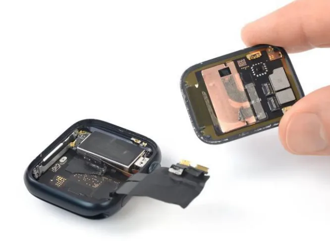
1) Smartwatches: Balancing High Integration and Reliability
Smartwatches utilize rigid-flex printed circuit board (PCB). The main board employs 0.8mm thick FR-4 material (Tg ≥ 150°C) to ensure thermal resistance, while the flexible connection sections use PI substrate (bending radius ≥ 8mm). Component layout requires clear functional zoning, such as maintaining ≥2mm spacing between power management, the main MCU (e.g., STM32L476), wireless chips (e.g., nRF52832), and sensors (e.g., MAX30102) to minimize interference. For assembly, the main board employs conventional reflow soldering, while the flexible section uses low-temperature solder paste. IPX7 waterproofing is achieved through a nano-scale waterproof coating (8μm) and silicone sealing.
2) Wireless Earbuds: Ultimate Miniaturization and Vibration Resistance
The PCBA of wireless earbuds pursues extreme miniaturisation, typically employing an ultra-thin (0.6 mm thick) rigid FR-4 PCB with an area of less than 5 cm². Key design features include a centrally positioned Bluetooth SoC (e.g. DA14531), surrounded by 01005-packaged passive components. To enhance vibration resistance, the solder joints of the components require underfill adhesive (e.g. Loctite 3609). The assembly process uses high-precision placement machines and controls the peak soldering temperature at 220°C. This is followed by AOI and X-ray inspection. For waterproofing, a 5μm nano-coating is applied over the entire unit, combined with silicone O-rings to achieve IPX4 protection.
3) Medical Patches: Flexibility, Bio-compatibility, and Long-Term Stability
Medical patches (e.g., continuous glucose monitoring) require fully flexible PCB (FPC) with a 0.1mm-thick polyimide (PI) substrate certified for bio-compatibility per ISO 10993-5. Layout follows a “flexibility-first” principle, with components arranged along edges and a minimum bending radius of ≥5mm. Ultra-low-power MCU (e.g., MSP430) and Bluetooth chips (e.g., nRF52805) enable up to 14 days of battery life. Assembly ensures the PCB perfectly conforms to body contours and passes bio-compatibility testing.
4) Finger Sensors: Flexible Wearable and Motion Capture
The finger sensor uses flexible PCB material and can be worn on the finger. It captures position and rotation angle data through motion amplitude. Its design prioritises miniaturisation and wearability, making it ideal for developing interactive functions such as gesture control. During assembly, ensure the flexible PCB’s bending durability and integrate high-precision sensors.
5) Sleep Monitors: Non-Contact Health Monitoring
The sleep monitor employs radar technology for non-contact monitoring. The PCB must integrate a radar module, light sensor, and low-power communication module (e.g., Air700E). During assembly, ensure the radar is installed at a 45° downward angle and positioned 1.5–2.5 meters from the subject. PCB design must optimize signal interference mitigation, with data acquisition and transmission handled via firmware.
5. Common Issues and Solutions in Wearable PCB Assembly
Wearable PCB assembly faces more complex manufacturing challenges than traditional PCBA due to demands for miniaturization, flexibility, and high reliability. By optimizing placement processes, soldering parameters, and substrate treatment, the yield and reliability of wearable PCB assembly can be effectively enhanced.
5.1 Insufficient Placement Accuracy for Ultra-Small Components (01005/0201)
1) Problem Manifestation: Component misalignment (>0.05mm offset), missing parts, or tombstone after placement, leading to soldering short circuits or open circuits, with yield rates often below 90%.
2) Core Causes:
Component Recognition Difficulty: 01005 components are minuscule (only 1/5 the size of a grain of rice), making traditional single-camera vision positioning prone to recognition errors.
Placement Pressure Control Difficulty: Components are extremely lightweight (e.g., 01005 resistors weigh approx. 0.001g). Excessive pressure (>50g) crushes components, while insufficient pressure (<20g) fails to secure solder paste.
Uneven Solder Paste Printing: Ultra-small component pads have minimal surface area (e.g., 01005 pads measure approximately 0.2mm × 0.15mm). Screen stencil aperture inaccuracies (deviations >0.005mm) cause abnormal solder paste volume.
3) Solutions:
Employ “dual-camera + 3D vision” placement machines (e.g., Fuji NXTP III) to enhance positioning accuracy to ±0.005mm.
Set placement pressure based on component type (01005 components: 20-30g; 0201 components: 30-40g), paired with flexible nozzles (silicone material, 0.2mm diameter).
Employ electroformed stencils (opening accuracy ±0.003mm) and ultra-fine-particle solder paste (alloy powder diameter 20-38μm), controlling printing speed at 20-30mm/s.
5.2 Flexible PCB (FPC) Soldering Prone to Deformation and Breakage
1) Problem Manifestation: During FPC soldering, high temperatures (traditional reflow soldering peaks at 230°C) cause substrate deformation (bending >1mm) and circuit breakage, with yield rates often below 85%.
2) Core Causes:
Poor Heat Resistance of Flexible Substrates: PI substrates have a glass transition temperature (Tg) around 280°C, but prolonged exposure to high temperatures (>200°C) causes substrate aging.
Soldering Stress Concentration: FPCs are thin (0.1-0.2mm) and have mismatched thermal expansion coefficients with components (e.g., component TCO 10ppm/°C vs. FPC approx. 50ppm/°C).
Difficulty in Fixing Flexible PCBs: FPCs are flexible and prone to bending, making stable fixation during soldering impossible compared to rigid PCBs.
3) Solutions:
Employ low-temperature soldering processes (peak temperature ≤200°C), such as Sn42Bi58 low-temperature solder.
Use specialized fixtures to secure FPCs, preventing displacement during soldering; incorporate stiffening plates or localized rigidification during design.
5.3 Solder Paste Printing and Soldering Defects
1) Common Issues: Abnormal solder paste volume (excessive/insufficient), paste misalignment, bridging, cold solder joints, short circuits, etc.
2) Inspection and Resolution:
Solder Paste Printing Inspection: Utilizes 3D SPI (Solder Paste Inspection) with ±0.001mm precision. Standard requires solder paste volume deviation ≤±15%.
Soldering Inspection:
Visual Inspection: AOI inspects solder joint appearance (e.g., solder balls, voids). Standard requires bright solder joints with no solder balls (diameter <0.1mm).
BGA Inspection: Utilizes X-ray inspection equipment (resolution 0.01mm). Standard requirement: Solder balls must be void-free (void area <20%).
5.4 Substrate Dimensional Stability Issues
1) Common Issues: Substrate dimensional changes, warpage (BOW), or twist (TWIST) affect subsequent routing and assembly precision.
2) Solutions:
Determine the substrate’s longitudinal and transverse shrinkage patterns and perform precise compensation before photolithography.
Control plating pressure; prioritize chemical cleaning or electrolytic processes for thin substrates.
Bake the substrate before drilling (temperature 120°C, duration 4 hours) to ensure complete resin curing.
5.5 Other Common Faults and solutions
Short Circuit: Inspect pad design and component orientation. Use a multimeter to measure resistance values and locate the short circuit point.
Open Circuit: Visually inspect for cracks. Use a multimeter to measure high resistance states. Employ the segment isolation method to narrow down the fault area.
Signal Integrity Issues: Use an oscilloscope to examine waveforms. Adjust circuit layout to minimize interference.
6. Future Development Trends of Wearable PCBA
The future development of wearable PCB assembly will focus on four key areas: miniaturisation, flexibility, high integration and green manufacturing. These areas will benefit from emerging technologies such as AI and smart vehicles.
1) Technological Advancements: Concurrent Development of High Density and Flexibility
Wearable devices impose stringent demands on PCB size, weight, and reliability, propelling technological progress in the following areas:
High-Density Interconnect (HDI) Technology: Utilizing laser drilling and blind/buried via techniques to reduce line widths below 10μm, supporting complex chip functionality while meeting device miniaturization requirements.
Flexible Printed Circuit (FPC): Increasing penetration in smart wearable, while foldable screen devices drive breakthroughs in FPC-HDI integration, enabling higher-layer counts and thinner designs.
Material Innovation: Adoption of high-frequency, high-speed materials (e.g., low-dielectric loss copper-clad laminates) ensures signal integrity, while eco-friendly materials like bio-based resins target a 30% substitution rate.
2) Application Scenarios: AI and Automotive Electronics Driving Demand
AI Hardware: Iterations of large AI models boost computing power requirements for wearable devices, increasing demands for PCB integration and complexity, driving growth in high-end products like HDI boards.
Automotive Electronics: Smart cockpits and ADAS systems promote FPC adoption in wearable devices (e.g., smartwatches, health monitors), significantly increasing PCB usage per vehicle.
3) Green Manufacturing: Environmental Protection and Sustainable Development
Process Optimization: Lead-free process coverage reaches 95%, while zero wastewater discharge technology achieves 90% copper ion recovery, reducing environmental costs.
Energy Management: Photovoltaic power generation exceeds 20% of total generation, with energy consumption per unit output decreasing by 18%, meeting global ESG standards.
7. Wearable PCB Assembly FAQs
When selecting materials for wearable PCBA, factors such as device flexibility requirements, operating environment, and cost must be comprehensively considered. Polyimide and flexible substrate materials are preferred choices for wearable devices due to their outstanding flexibility and reliability.
Wearable PCBA requires full-process inspection (SPI→AOI→X-Ray) to ensure quality, while relying on high-precision placement equipment to achieve miniaturized production.
Substrate Treatment: Utilizing low-surface-energy materials like polypropylene (PP) film effectively prevents moisture penetration while maintaining breathability.
High-melting-point Solder: In high-temperature environments, prioritize gold-tin solder (melting point 280°C) to ensure joint stability under heat and prevent circuit interruptions caused by solder joint failure.
Conformal Coating Application: Polyurethane (PU) coatings are recommended due to superior moisture resistance and mechanical stress tolerance compared to acrylic or epoxy resins, effectively isolating moisture and corrosive substances.
Interface Protection: All external interfaces (e.g., USB, charging ports) employ dual protection with rubber plugs + silicone brackets, reinforced by interference fits and screw fasteners to enhance sealing integrity.
Reduce Through-hole Components: Prioritize SMT components to lower manual soldering costs.
Trace Width and Spacing: Design trace widths based on current requirements to prevent signal interference and overheating.
Material Selection: Use specialized substrates (e.g., low-dielectric constant materials) for high-frequency signals to avoid signal distortion.
Heat Dissipation Design: Add copper heat sinks to high-current traces to prevent cold solder joints.
Use low-temperature solder paste (e.g., Sn63Pb37) and control peak reflow temperature below 200°C to prevent substrate deformation.
Bake FPCs (120°C, 4 hours) to remove moisture before soldering, and use specialized fixtures for stress relief.
Increase Copper Pour Area: Apply large copper pours for power and ground traces to rapidly dissipate heat through copper sheets, reducing localized hotspot temperatures.
Optimize Pad Design: Ensure package pin pads are larger than chip pins to increase solder contact area, enhancing thermal conductivity and reducing the risk of cold solder joints.
8. Summary
Wearable PCB assembly is a “scenario-driven” process that requires specialized optimization in dimensions, reliability, and flexibility to meet the core demands of human wearability and satisfy the practical usage requirements of the device. Each technical challenge in wearable PCB assembly must be addressed in conjunction with the “miniaturization and flexibility” characteristics of wearable devices to achieve high yield and high-reliability assembly outcomes.
Table of Contents

Get Your PCB Quote!


