
A Complete Guide to Wave Soldering and Reflow Soldering
Wave soldering and reflow soldering are the two main soldering processes in electronic manufacturing.
Get Your PCB Quote!
Table of Contents

In the field of electronic manufacturing, wave soldering and reflow soldering are two common soldering processes. They play an important role in achieving the connection between electronic components and circuit boards. There are significant differences between the two in terms of working principles, application scenarios, advantages and disadvantages, etc.
1.Soldering Overview
1.1 What is Soldering?
Soldering is the technique of attaching electronic components to pads on a PCB or printed circuit board. Wave soldering and reflow soldering are different soldering methods. Solder is an alloy that melts at low temperatures and, in its molten state, forms a metallurgical bond between the component leads and the copper pads on the PCB. Upon cooling, the solder hardens, forming a mechanically rigid and electrically conductive bridge between the pad and the component lead. The mechanical rigidity of the solder allows it to hold the component in place, while its electrical conductivity enables the component to function properly in a circuit.

1.2 How to Solder?
Soldering requires heating to melt the solder and flow it, then cooling to resolidify it. Traditionally, technicians use a soldering iron to heat it and use periodic convection to cool it. They apply the hot tip of the electric soldering iron to the pads and component pins while applying solder and flux to the hot surface. The flux acts as a reducing agent here, because most metals will form an oxide layer on the surface that cannot be soldered under the action of heat and oxygen in the surrounding atmosphere. The heat melts the solder, causing it to flow along the hot surface, forming a metallurgical bond. As the solder cools, it solidifies and firmly bonds the component to the copper pad.
However, the above process requires heating each solder joint individually for soldering. The process is slow and laborious. In addition, the formation of the solder joint depends on the skill of the operator, and there may be differences in quality between solder joints. In order to achieve high-volume production and obtain high-quality and stable solder joints, the electronics industry relies on automated soldering processes, of which there are two main types.
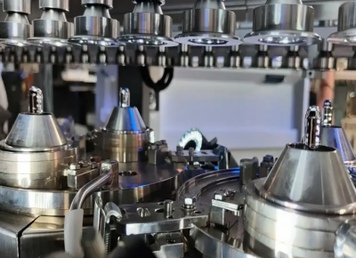
2.What is Wave Soldering?
Wave soldering is a batch soldering process that can solder a large number of circuit boards in a very short time. A conveyor belt carries each assembled circuit board to a pan or tank containing molten solder. A pump in the pan or tank drives the molten solder through a nozzle, forming a solder wave. The solder wave contacts the bottom of the circuit board and component leads as it passes over the circuit board and partially adheres to the leads. As the circuit board passes, it cools naturally or is forced to cool by blowing air. After cooling, the molten solder hardens and fixes the component in place.
2.1 Principle of Wave Soldering
Wave soldering injects molten solder (lead-tin alloy) through an electromagnetic pump or nitrogen to form a dynamic solder wave, so that the PCB with pre-installed components passes through the wave to achieve mechanical and electrical connection between the solder end and the pad. The core process includes a double-wave structure:
Turbulent Wave: break the oxide film and initially wet the solder joint;
Laminar Wave: complete the final soldering and correct the shape of the solder joint.
2.2 Process Flow and Parameter Setting
1) Preparation Stage
PCB Pretreatment: The solder mask or high-temperature resistant tape is applied to the welding surface to protect the gold finger and the jack; larger slots need to be blocked to prevent tin leakage.
Flux Spraying: spray evenly to the bottom surface of the PCB to ensure that a small amount of penetration from the through-hole to the pad (the component body cannot be touched).
2) Preheating
Temperature: 90–130℃ (upper limit for thick boards/high-density SMD boards), heating rate ≤3℃/second.
Function: Evaporate flux solvent to avoid tin explosion; reduce thermal shock and prevent PCB deformation.
3) Soldering
Crest Temperature: 220–250℃ (the actual temperature of the tin furnace is 5–10℃ higher than the crest).
Crest Height: more than 2/3 thickness of the bottom surface of the PCB.
Transmission Speed: 0.8–1.92 m/min, to ensure sufficient contact time of the solder joint.
4) Cooling and Post-processing
Forced Cooling: air cooling or water cooling (rate 4–6℃/second), solidifies the solder joint and enhances strength.
Pin Cutting: The length of the component pin is retained at 1.4–2.0mm.
2.3 Key Equipment Operation Specifications
1) Start-up Preparation
Check the air pressure (≥0.5 kg/cm²), the specific gravity of the flux, and the liquid level of the tin furnace (supplement the solder when it is 15mm lower than the tin furnace).
Remove tin slag and add antioxidants.
2) Production Monitoring
Real-time observation of flux coverage uniformity, wave peak stability, and solder joint quality.
Quality inspection is required after each PCB is soldered, and defective boards are immediately re-soldered or parameters are adjusted.
3) Shutdown Maintenance
Clean the nozzle welding slag daily, and calibrate the temperature sensor and electromagnetic pump regularly.
2.4 Common Defects and Solutions
| Defect Type | Main Cause | Solutions |
| Solder Bridging/Solder Beading | Temperature is too low, transmission is too fast, insufficient flux | Increase the temperature to 240℃, reduce the speed, and increase the amount of flux |
| Pseudo Soldering/Cold Soldering | Insufficient preheating, component oxidation | Preheating temperature>120℃, check the solderability of the pins |
| Solder Beads | Flux contains water or the PCB is stained with solder paste | Replace the flux and clean the PCB |
| Insufficient Through-hole | Insufficient wave crest height, turbulent wave failure | Adjust the wave crest height and clean the nozzle |
2.5 Precautions
Protective Measures: Operators must wear welding helmets and heat-resistant gloves, and the work area must be well ventilated.
Environmentally Friendly Process: Use lead-free solder and nitrogen protection welding (oxygen content ≤ 100ppm) to reduce oxidation.
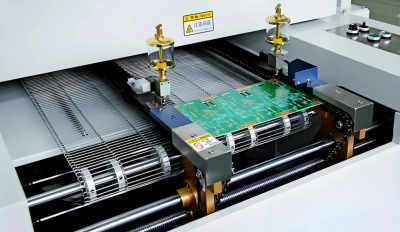
3.What is Reflow Soldering?
Reflow Soldering is another batch soldering process that is also suitable for soldering a large number of circuit boards in a short period of time. However, this process is only suitable for SMT (Surface Mount Technology) components, which are very small and most of them do not have leads. Instead of using a can of molten solder, reflow soldering requires applying solder paste to the PCB pads before mounting the SMT components. Then, the SMT components, which are located on a thin layer of solder paste, will be reflow soldered.
3.1 Basic Principles of Reflow Soldering
Reflow soldering can be completed by precisely controlling the temperature curve, which is divided into four stages:
1) Preheating Zone (Room Temperature→150℃)
Slowly increase the temperature (1-3℃/second) to evaporate the solder paste solvent and prevent the tin beads from splashing; activate the flux and clean the oxide on the surface of the pad.
2) Insulation Zone (150-190℃)
Preheat at a constant temperature for 60-90 seconds to eliminate the temperature difference between the component and the PCB and avoid thermal stress damage.
3) Reflow Zone (Peak Temperature 217-250℃)
Solder paste melts (the melting point of lead-free solder paste is 217-220℃), and the liquid tin wets the pad to form a reliable solder joint, and the time is controlled within 30-60 seconds.
4) Cooling Zone
Rapid cooling (≤4℃/second) to solidify the solder joint. Cooling too quickly can easily cause cracks in the component.
3.2 Standard Operating Procedures
1) Equipment startup and preheating
Turn on the main power supply and exhaust system, start the reflow soldering machine, and log in to the control system.
Call the pre-stored temperature curve (for example, eight-zone lead-free program: 165℃→160℃→175℃→185℃→190℃→190℃→240℃→200℃).
Turn on the air supply, conveyor belt, and heating system, and preheat for 20-30 minutes until the actual temperature (PV) and the set value (SV) are stable.
2) Parameter Calibration and Testing
Use a thermometer to measure the furnace temperature, and adjust the abnormal temperature zone SV value or conveyor belt speed (standard 75±10cm/min).
3) Production Operation
PCB Preparation: Clean the pad and check for deformation, apply an appropriate amount of solder paste (avoid excessive).
Component Mounting: Accurate installation, ensure correct polarity.
Furnace Soldering:
Single-sided mounting: pre-apply solder paste → mounting → reflow soldering.
Double-sided mounting: small first, then large; light first, then heavy components.
Cooling Inspection: remove the solder joint after solidification, and check the soldering integrity and surface finish.
4) Shutdown Steps
First, turn off the heating system, wait for the equipment to cool for 30 minutes, then turn off the air supply and conveyor belt.
Turn off the computer power, and finally turn off the main power switch.
3.3 Common Problem Solving
| Defects | Cause Analysis | Solution |
| Tombstoning | Uneven preheating/unbalanced solder paste tension | Reduce heating rate; adjust solder paste printing thickness |
| Solder Beads | Too fast heating or solder paste moisture absorption | Fully preheat; seal and store solder paste |
| Pseudo Soldering/Solder Insufficient | Insufficient solder paste or too low temperature | Expand steel mesh aperture; calibrate reflow zone temperature |
| Voids in Solder Joints | Too fast cooling or residual contaminants | Optimize cooling curve; strengthen PCB cleaning |
3.4 Precautions
Personal Protection: Wear heat-resistant gloves, goggles, and anti-static clothing.
Environmental Requirements: Good ventilation, away from flammable materials; it is forbidden for one person to operate multiple devices.
Emergency Treatment: Press the emergency stop switch immediately in case of abnormal smoke or noise.
First Article Inspection(FAI): Check the gloss and shape of the solder joint (semi-elliptical shape is preferred), and remove solder balls or residues.
Regular Temperature Measurement: Use a thermometer to verify the actual curve matching standard (tolerance ±5℃) every day.
Equipment Maintenance: Confirm that the emergency brake switch is effective and the track is not blocked by debris; clean the flux residue every week and calibrate the sensor accuracy.
4.Comparison of Wave Soldering and Reflow Soldering
Reflow soldering achieves SMT soldering by “discharging materials first and then melting”, while wave soldering completes THT soldering by “dynamically contacting liquid tin”. The two complement each other in electronic manufacturing.
4.1 Different Process Principles
Reflow Soldering:
Through preheating, reflow, cooling, and other stages, the solder paste pre-coated on the PCB pad is heated to melt and combine with the pins of the mounted components, and then form solder joints after cooling. The whole process does not require direct contact with liquid solder.
Wave Soldering:
The molten solder forms a continuous wave through the nozzle, and the PCB carries the plug-in components through the wave at a specific angle. The solder covers the pins and cools and solidifies. The pins need to pass through the PCB through-hole to achieve soldering.
4.2 Different Applicable Components
Reflow Soldering:
Specially used for surface mount components (SMD), such as chip resistors, capacitors, BGA packaging, etc., supporting high-density integrated design.
Wave Soldering:
Applicable to through-hole components (THT), such as connectors, transformers, or integrated circuit sockets with pins.
Note: Double-sided PCB requires reflow soldering of SMD components first, and then wave soldering of THT components.
4.3 Different Process Parameters
| Parameters | Reflow Soldering | Wave Soldering |
| Soldering Temperature | 150°C–260°C (multi-zone precise temperature control) | 240°C–280°C (single peak high temperature contact) |
| Solder Carrier | Solder Paste (Solid + Flux) | Liquid molten solder (pure tin/alloy) |
| Thermal Stress Effect | Small (uniform heating) | Large (local sudden heating) |
| Environmental Protection | Low volatility (flux sealing) | Flux exhaust gas needs to be treated |
4.4 Different Welding Quality and Efficiency
Reflow Soldering: The temperature curve is precisely controllable, the solder joints are uniform and have few voids, and the degree of automation is high, which is suitable for miniaturized products (such as mobile phone motherboards).
Wave Soldering: Batch soldering has high efficiency, but it is easily affected by the wave crest shape and PCB inclination, which may cause bridging or leakage.
4.5 Different Application Scenarios
Reflow Soldering: Consumer electronics (mobile phones, computers), high-density SMT boards, and double-sided mounting scenarios.
Wave Soldering: Industrial control, automotive electronics, power boards, and other fields with large plug-in components, as well as cost-sensitive large-scale production.
4.6 Different Development Trends
Reflow Soldering develops towards precision technologies such as vacuum soldering and nitrogen protection to reduce oxidation defects.
Wave Soldering is optimized to selective wave soldering, which precisely solders specific through holes by moving the tin nozzle to reduce thermal damage and solder waste.
5.Advantages and Disadvantages of Wave Soldering and Reflow Soldering
5.1 Advantages and Disadvantages of Wave Soldering
1) Wave Soldering Advantages:
High Efficiency and Economy
Suitable for welding large quantities of plug-in components (such as transformers and connectors), and can complete multi-pin welding at the same time, significantly improving production capacity; low equipment cost and maintenance cost, suitable for large-scale production.
Compatible with Plug-in Components (THT)
Supports stable welding of through-hole plug-in components, has strong adaptability to large components, and is irreplaceable in industrial control, automotive electronics, and other fields.
2) Wave Soldering Disadvantages:
Welding Quality Fluctuation Risk
Solder oxidation, PCB deformation, or unstable wave shape can easily lead to defects such as bridging and cold soldering, and process parameters need to be strictly controlled.
Limited Application Scope
Only applicable to plug-in components, surface mount components (SMD) cannot be welded; PCB size and shape are limited by the tilt angle of the equipment.
Environmental Protection and Material Challenges
Traditional lead-containing solder has the risk of pollution, and the lead-free process requires a higher welding temperature (240–280℃), which has strict requirements on component heat resistance.
5.2 Advantages and Disadvantages of Reflow Soldering
1) Reflow Soldering Advantages:
High Precision and Stability
After the solder paste melts, it self-calibrates its position through surface tension, which is particularly suitable for micro high-density components (such as chips and resistors) and has a low soldering defect rate.
Automation and Environmental Protection
Fully automated production lines improve efficiency; the mainstream uses lead-free solder paste, which meets environmental standards.
Wide Compatibility
Supports various surface mount components (SMD), suitable for precision electronic products such as mobile phones and computers, and can be expanded to double-sided mounting processes.
2) Reflow Soldering Disadvantages:
High Cost Investment
The reflow oven and temperature control system equipment are expensive, and the solder paste storage and printing process require strict environmental control, which increases production costs.
Process Complexity
The temperature curve (preheating, heating, cooling) needs to be precisely designed, and the operator needs professional technical experience.
Oxidation Sensitivity Issues
When ordinary reflow ovens are operated in the air, high temperatures easily oxidize solder joints, and nitrogen protection (nitrogen reflow ovens) is required to ensure high-reliability welding.
6.Wave Soldering &Reflow SolderingFAQs
Reflow Soldering: Melt the solder paste pre-printed on the pad and form solder joints through hot air or infrared heating, which is suitable for surface mount components (SMT).
Wave Soldering: Use molten solder to form a wave crest, and the plug-in component (THT) pins contact the liquid solder to complete the soldering.
Reflow Soldering: Designed for SMT, such as small and high-density components such as chip resistors, capacitors, and IC chips.
Wave Soldering: Mainly used for through-hole components (THT), such as transformers, connectors, and other pin-type components; under special processes, a small amount of SMT can be compatible.
Chip components are small and need to be fixed first, while plug-in components are larger. First complete SMT reflow soldering, then THT wave soldering, to prevent small components from being washed away or shifted by liquid solder.
Choose Reflow Soldering: high-density SMT boards (such as mobile phones and computer motherboards), which require precise temperature control and miniaturized soldering.
Choose Wave Soldering: PCBs with a large number of plug-ins (such as home appliances and automotive control panels), with high batch production efficiency.
Reflow soldering cannot directly solder plug-in pins.
Wave soldering is compatible with a few high-temperature resistant SMT components (such as specific package inductors), but requires customized processes and has a higher yield risk.
Temperature Increase:
The melting point of lead-free solder (such as Sn-Ag-Cu) increases, and the peak value of reflow soldering needs to reach 240–260℃, and wave soldering needs to be above 260℃.
Defect Control:
Lead-free solder has poor wettability, and it is necessary to optimize flux activity and nitrogen protection (oxygen content <500ppm) to reduce tin beads/false solder joints.
Reduce Oxidation: Reduce oxygen content to <1000ppm (ideally <500ppm) to improve solder joint wettability.
Improve Quality: Especially for lead-free soldering, the void rate can be reduced by more than 30%.
7.Summary
Wave soldering and reflow soldering are the two main soldering processes in electronic manufacturing. Wave soldering uses molten solder waves to solder plug-in components, which is suitable for through-hole components; Reflow soldering achieves surface mount components (SMD) soldering by heating pre-printed solder paste, which has the characteristics of high precision and low thermal shock. The two are complementary in PCB assembly to jointly ensure the reliable connection of electronic products.
With the rapid development of electronic technology and fierce market competition, it is very important to choose a reliable partner. As an experienced manufacturer with excellent capabilities in PCB fabrication, PCB assembly, and components sourcing service, we provide customers with one-stop solutions for electronics needs. With advanced equipment, strong technical force, and perfect quality assurance system, our company can ensure high-quality products and fast delivery time. Whether you are looking for high-volume production or prototype services, we will meet your requirements with competitive prices and on-time deliveries. Welcome to send us Gerber files and BOM lists for a cost-effective quotation!
Table of Contents

Get Your PCB Quote!


