
PCB Prototype Board Guide: Optimize Design & Reduce Costs
From design optimization to accelerated production to cost control, the value of the PCB prototype board is evident throughout the entire process.
Get Your PCB Quote!
Table of Contents
PCB prototype board is not only “design verification tools” but also “the litmus test for manufacturing processes.” Making a lot of PCBs involves doing many things, like soldering, putting in components, and putting everything together. Some design choices might not work well with how things are actually made. For example, if the spaces between parts are too small, it can be hard to solder them. Also, if the board is too thick, it might not meet the factory’s standards. And if there are too many vias, it can slow down production. These issues require early adaptation through PCB prototyping.
1. What is a PCB Prototype Board?
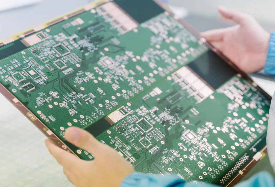
A prototype PCB is a sample of an electronic product that is used to test the design and see if it can be made. Most prototypes are made to test how easy it is to use, but PCB prototype boards must also work a little because they are made to check how well the design works. During the PCB prototyping process, engineers can experiment with different PCB designs and manufacturing specifications to identify the most effective approach.
2. What are the Benefits of PCB Prototyping?
2.1 Reducing Project Timelines
During PCB design, engineers undergo multiple iterations before finalizing the PCB product, often resulting in extended timelines. PCB prototyping accelerates the entire design and manufacturing process by:
1) Comprehensive testing to promptly identify and address defects
PCB prototype boards enable PCB design engineers to swiftly and accurately test design issues. Omitting this step prolongs the time required to uncover design flaws. Failure to deliver on time may lead to customer dissatisfaction and result in lost revenue.
2) Early Product Preview for Enhanced Client Communication
Clients often request product visibility at multiple production stages. Providing prototypes facilitates clearer design communication, minimizes client interactions, and reduces redesign requests.
3) Minimize Rework
PCB prototyping allows pre-production inspection and testing, significantly reducing rework. Defective boards entering production incur prolonged timelines and increased costs.
2.2 Improving PCB Production
When utilizing third-party PCB prototyping services, selecting an effective communicator is essential. Several factors during the design process can lead to errors, including:
1) Excessive revisions without timely communication, making it difficult to identify the optimal version.
Design changes driven by client requests or shifts in the design team can result in accumulated and overlapping PCB versions. Inadequate documentation then prevents the final version from being clearly identified and confirmed. Additionally, compromises made to meet client demands may overshadow optimal design choices.
2) Design Blind Spots
Designers may excel in specific PCB types but lack expertise in others, potentially introducing minor flaws.
3) Design Rule Checks (DRC)
While DRC tools effectively detect obvious design issues, they have limitations. For example, DRC can check if there are ground return paths, but it can’t decide on the best way to route things, including the size and length of the paths. This means it can’t create the best possible path.
These three issues together lead to inefficiency, problems in the design, and other oversights during the review process. Some companies that make prototypes use methods to deal with these problems. This allows them to suggest design improvements before starting to make prototypes. This ensures the PCB prototype board is better suited for the testing process.
2.3 Pre-testing PCB Functionality
Having accurate and reliable PCB prototypes makes it easier to solve design issues during the development process. High-quality PCB prototypes show how the final product will work. This lets engineers check and test the following parts:
1) PCB Design
Prototyping helps engineers identify defects early in the development process. If the design is more accurate, it will be easier to identify defects. This will reduce design costs and shorten project timelines.
2) Functional Testing
PCB prototype boards enable engineers to inspect and evaluate specific product functions. Some concepts that appear theoretically sound may prove ineffective in practice. Accurate PCB boards facilitate the assessment of theoretical values against actual performance.
3) Environmental Testing
Many products must operate in specialized environments, necessitating appropriate PCB testing to ensure reliable performance under such conditions. For instance, prototypes typically undergo temperature variation testing, power fluctuation testing, and shock resistance testing.
4) Final Product Design
PCB prototype boards help determine whether adjustments to the planned product or packaging are needed for the final PCB design.
For these purposes, accurate PCB prototype boards significantly streamline other processes and enable engineers to prepare comprehensively for production planning.
2.4 Testing Individual Components
Engineers often use PCB prototype boards to test their designs. The most valuable tests are the ones that evaluate individual components and functions. The main focus of prototype PCB testing is to check that each feature on the PCB is working the way it should. This type of testing serves multiple purposes, including:
1) Validating Design Concepts
Simple PCB prototype boards are used to test the ideas behind a design before the design is developed further. Engineers can verify if the design is viable and, if not, quickly pinpoint where issues arise.
2) Breaking Down Complex Designs
Simple PCB prototype boards are used to test the basic parts of the final PCB. This makes sure that it will work before moving on to the next design phase. Step-by-step testing helps identify design issues incrementally, enabling faster and more precise adjustments. The isolated testing approach allows engineers to test individual functions effectively and efficiently.
2.5 Reducing PCB Manufacturing Costs
Standard PCB production runs are costly, making prototyping crucial for lowering manufacturing expenses. Prototypes help engineers address and prevent the following issues:
1) Identifying Design Flaws
The earlier engineers detect design flaws, the sooner they can fix them at lower costs. Delayed detection leads to higher remediation expenses. If issues persist into full-scale production, they can severely disrupt budgets.
High-quality PCB prototyping services enable rapid and accurate detection and resolution of design flaws, ultimately reducing costs over the long term.
2) Determining Product Adjustments
In some cases, changes to the PCB might cause slight deviations from the original shape or material. This could affect the whole product’s specifications and manufacturing needs.
PCB prototype boards can determine if early product adjustments are necessary. This improves planning and reduces costs associated with redesigning the product and its packaging.
In short, PCB prototyping helps make products better while lowering costs during manufacturing.
3. What are the Manufacturing Specifications of PCB Prototype Board?
3.1 Dimension
This is straightforward: the PCB’s physical size. PCB costs scale with surface area, so it’s important to make the most of space to save money. Also, irregularly shaped PCB designs waste material during manufacturing, and smaller rectangles on the same PCB board cost more.
Single-board Design Dimensions: Common ranges from 50mm*50mm (mini modules) to 300mm*200mm (industrial controllers), with 100mm*100mm being the most cost-effective prototyping size.
Production Substrate Dimensions: Standard copper-clad laminate sheet sizes include 457mm*610mm (18*24 inches) and 508mm*508mm (20*20 inches), with slight variations among manufacturers.
Equipment Limitations: PCB manufacturing facilities typically have a processing upper limit of 530mm*630mm (approximately 21*25 inches).
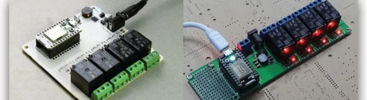
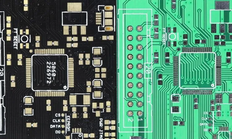
The relay shielding on the left version occupies an area of approximately 74.5 cm², leaving significant unused space. The second iteration PCB prototype board on the right reduces the footprint to 65.4 cm².
3.2 Layer and Thickness
Layer Range: 1–40 layers, with 1–6 layers common for prototyping.
Board Thickness Selection:
1) Standard Thickness: 1.6mm (used in over 80% of double-sided boards).
2) Special Requirements: 0.2mm–8.0mm, tolerance ±10% (t≥1.0mm) or ±0.1mm (t<1.0mm).
PCB manufacturers choose the core dimensions based on the number of copper layers to get the right board thickness. Confined spaces may necessitate 1.0mm or thinner boards. Manufacturers typically accommodate thicknesses as low as 0.4mm.
3.3 Material
Standard multilayer PCBs consist of several copper-clad laminates stacked together. The most common PCB material today is glass-reinforced epoxy, also called FR-4. “FR” stands for “flame retardant,” and the number indicates its flammability rating. However, you need to be careful when designing high-speed or RF boards because the material’s dielectric properties and thickness are important.
3.4 Surface Finish
Pad plating is a technique where the exposed copper surfaces of a PCB are coated with another metallic material to make it easier to solder during assembly. The most common plating technique is leaded or lead-free HASL (Hot Air Solder Leveling), which puts solder on the board during PCB assembly.
Another technique is ENIG (Electroless Nickel Immersion Gold) plating. This is a more expensive plating method, but it makes the surface more resistant to oxidation and more flat. This makes it an excellent choice for large BGA components and exposed contact pads or test points.
The PCB on the left is plated with ENIG, while the PCB on the right features standard HASL. Notice how the HASL pad is uneven, whereas the ENIG pad is perfectly flat.
3.5 Impedance Control
If a PCB contains radio components (Wi-Fi, Bluetooth, etc.), impedance control may need to be specified. Impedance control is a way to use predefined patterns (often RF networks) to create a known resistance to all signals that go through them.
Impedance is affected by many things, like the dielectric of prepreg materials, trace width, and solder mask. Controlling impedance is critical for optimizing wireless antenna performance. For example, Wi-Fi antenna circuits are typically controlled to 50 ohms impedance.
Impedance control requires expensive equipment, and not all manufacturers can guarantee controlled impedance. This can increase manufacturing costs, which rise further if tolerances for controlled impedance are relatively strict.
3.6 Minimum Width/Spacing
This refers to the minimum width of copper traces on a PCB and the minimum distance between traces. For 1 oz copper thickness, it is 2.5 mil/2.5 mil; for 2 oz copper thickness, it is 5 mil/5 mil.
The left board uses default width and spacing tolerances, while the right board requires tighter tolerances. Notice how the holes on the via are not perfectly centered. This becomes an issue when PCB manufacturers cannot meet their tolerances. Therefore, use as much copper as possible.
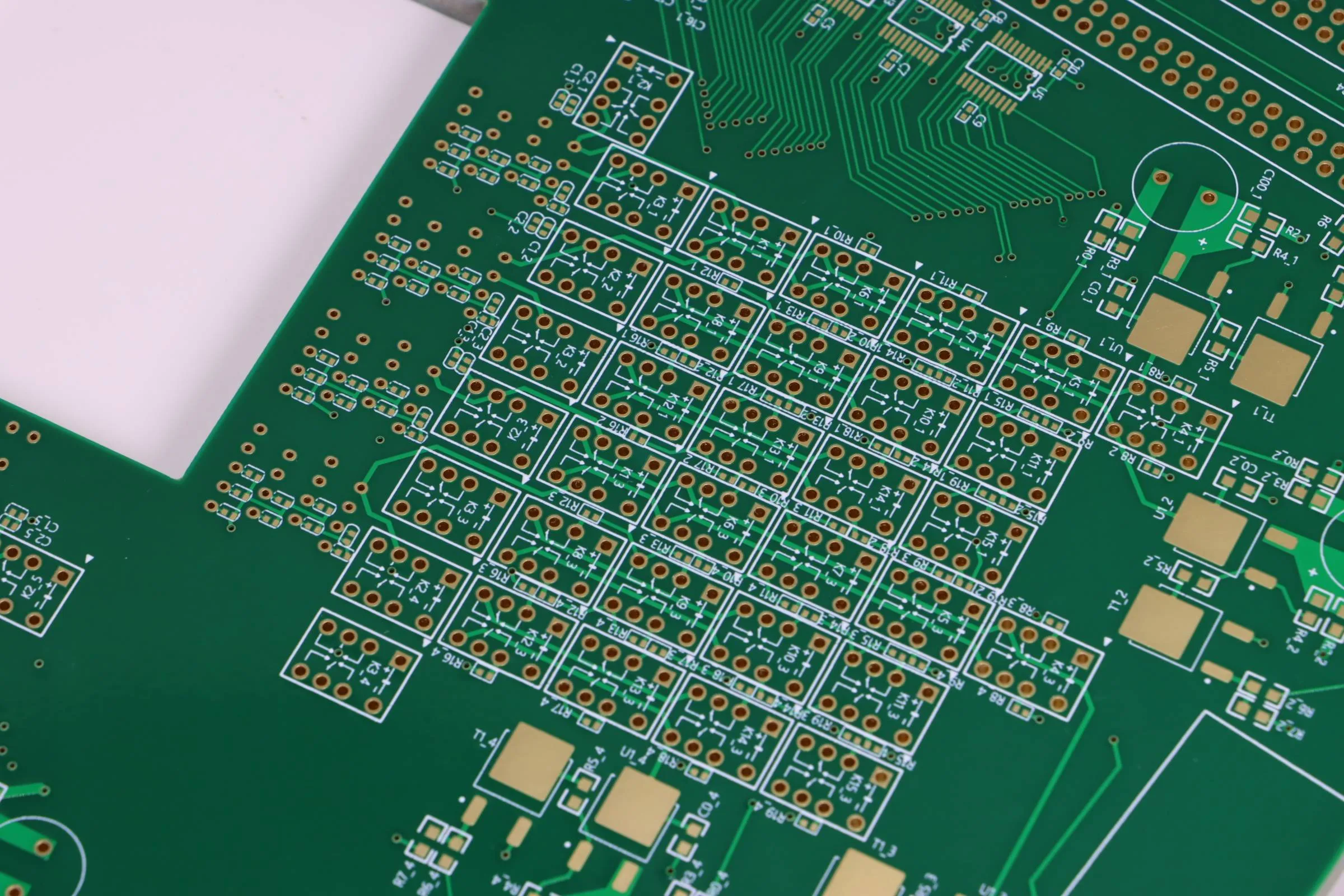
3.7 Holes and Vias
The size of holes and vias (vertical electrical connections between copper layers) on a circuit board. Specifying smaller pads and vias on a PCB is an effective way to save space, but it also increases manufacturing complexity. Smaller holes require tighter tolerances during drilling and generate more scrap material.
3.8 Solder Mask
The solder mask helps prevent solder bridges that could cause short circuits and is typically applied over the copper traces on a PCB. Beyond standard green, you can also choose red, yellow, blue, black, or white.
3.9 Silkscreen
Screen printing is used to record and annotate text, graphics, and symbols on PCBs. LPI printing (liquid photo imaging) is a more precise alternative to screen printing. It can produce screens with a higher resolution than screen printing, but it costs slightly more.
3.10 Minimum Pitch
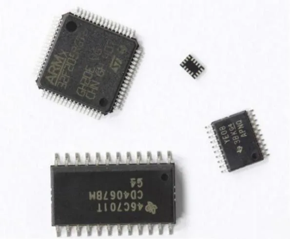
In the PCB field, “pitch” refers to the distance between adjacent pins on an electrical component. If a PCB requires complex components with numerous pins and very fine pitch, a higher-cost assembly facility may be necessary. If the pitch is too narrow, it can lead to a lower yield. This means that you should think about how much scrap is expected and how much it will cost.
Modern integrated circuits now offer virtually unlimited packaging options and pitch variations. QFN and BGA packages often present greater challenges during prototyping or hand-assembled circuit boards.
3.11 Notched Holes
If you are manufacturing a template or PCB that will be mounted onto another PCB, consider adding notched pads to your PCB design.
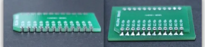
Left – PCB with serrated pads. Note the HASL copper plating (silver) on the PCB side. Right – PCB mounted onto the mainboard.
3.12 RoHS Compliance
If you manufacture PCBs, you should tell the manufacturer about your RoHS compliance requirements. This is a common requirement, but leaded and non-compliant components are still used often. These components can sometimes get put into designs if they are not explicitly specified.
4. PCB Prototype Board FAQs
1) What is a PCB prototype board?
A PCB prototype is a sample of an electronic product that shows how it will work and how well it will perform. Unlike regular prototypes, it must actually work like a circuit, which allows us to improve it by trying different design and manufacturing specifications.
2) What tools are commonly used to manufacture PCB prototypes?
Some of the software options are Altium Designer, Cadence Allegro, Mentor Xpedition (PADS Pro), KiCad, Eagle (Autodesk), EasyEDA, and so on.
3) What is the typical lead time for PCB prototyping?
How long it takes to make a PCB prototype depends on how complex the design is, how it’s made, and when the manufacturer is able to make it.
Simple single/double-layer boards Standard prototyping: 3-5 working days (including engineering review, production, and testing).
Multi-layer boards 4-6 layer boards: 5-8 working days (requires inner layer lamination, drilling, and other processes).
4) Which step is the most time-consuming in PCB prototyping?
The most time-consuming steps in PCB prototyping primarily occur during the manufacturing phase, particularly in the lamination and drilling processes for multilayer boards, which account for over 50% of the overall cycle time.
5) What should be considered in PCB prototyping?
PCB prototyping is a key step in developing electronic products. It involves strict control of the design, materials, manufacturing techniques, and testing processes.
6) How to control PCB prototype board manufacturing costs?
Employ functional zoning layouts to shorten trace lengths, reduce via counts, and avoid special processes like blind/buried vias.
Use standard hole sizes (≥0.2mm) and common components (e.g., 0805 resistors) to lower fabrication complexity.
You can choose 1 oz of copper instead of 2 oz, and focus on HASL or OSP surface finishes. These are cheaper alternatives to gold plating.
For small-batch prototyping, utilize scrap material (e.g., leftover 200mm×100mm boards) to reduce material costs to zero.
5. Summary
The PCB prototype board is important for the whole electronics R&D process. It helps confirm the design is correct and reduce the cost. It also quickly improves the design and makes the process better. It enables people to work together. It’s not an extra cost, but an investment that prevents greater losses. It’s not a step that delays progress, but an accelerator that shortens the time it takes to market a product. Making PCB prototyping a priority helps ensure better product development, smoother mass production, and a competitive edge in the marketplace.
Table of Contents

Get Your PCB Quote!


