
What is PCB Silkscreen?You Need to Know About Process & Polarity
In the field of modern electronic manufacturing, PCB silkscreen is an important link that cannot be ignored in the circuit board design and production process.
Get Your PCB Quote!
Table of Contents
- 1. Che cosa è la serigrafia PCB? (Definizione e funzioni)
- 2. Quali sono i tipi più comuni di serigrafia su PCB?
- 3. Perché utilizzare la serigrafia sui PCB?
- 4. Diverse tecnologie di serigrafia PCB e i loro vantaggi e svantaggi
- 5. Processo di stampa serigrafica su PCB: passo dopo passo
- 6. Considerazioni sulla progettazione della serigrafia PCB
- 7. Problemi comuni e raccomandazioni di progettazione per le marcature di polarità serigrafiche dei PCB
- 8. Domande frequenti sulla serigrafia PCB
- 9. Riassunto
In the modern electronics manufacturing industry, PCB silkscreen is a crucial and indispensable step in circuit board design and production. Screen printing not only enhances the readability and aesthetic appeal of PCBs but also provides significant convenience for subsequent assembly and maintenance processes. As a one-stop PCB manufacturer, explaining different types of screen printing and their functions to customers not only helps showcase product features and advantages but also strengthens client confidence in product quality and performance.
1. What is PCB Silkscreen?(Definition & Functions)

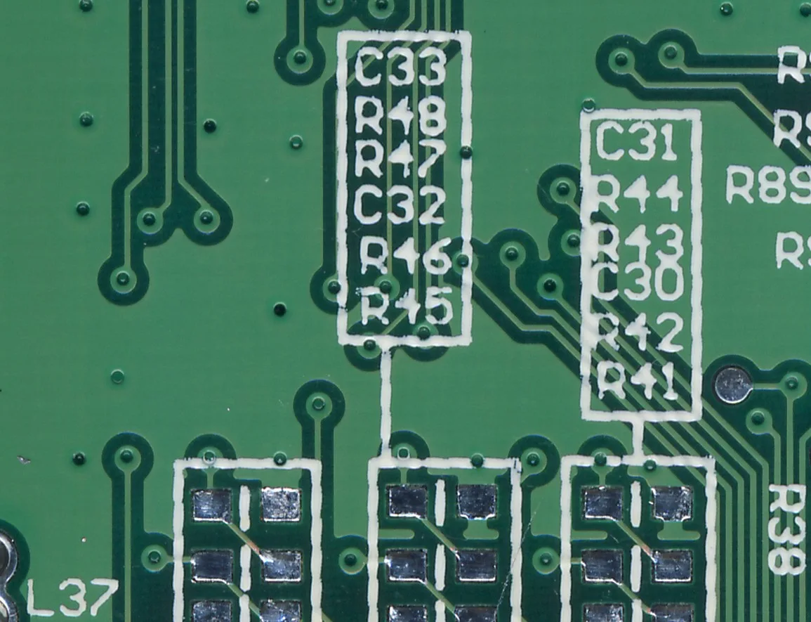
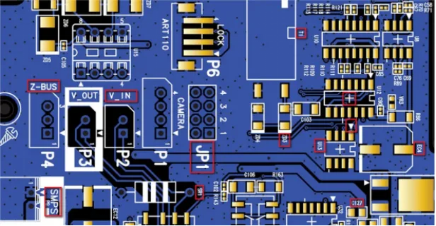
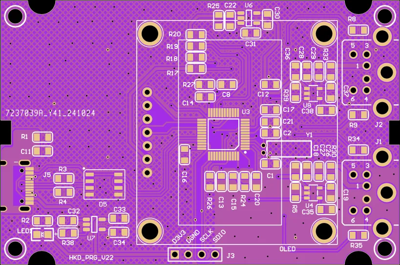
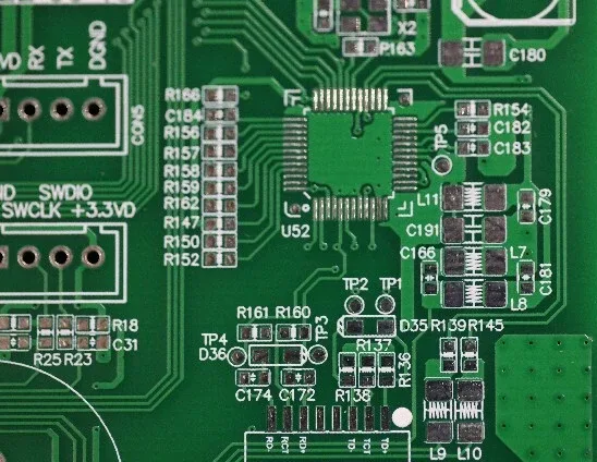
PCB silkscreen refers to the layer of text, symbols, or patterns printed onto the surface of a circuit board using screen printing technology. It is primarily used to identify non-electrical information such as component details, polarity markings, and test points. Its core functions include:
Marking Components
Enhance assembly efficiency and repair convenience by labeling component locations (e.g., R1, C2) and polarity (e.g., diode direction indicators) using alphanumeric combinations.
Tracing Production
Includes manufacturer logos, version numbers, production dates, and other details for quality tracking and brand display.
Indicating Function
Indicates interface types, safety warnings (e.g., high-voltage labels), and test point locations to assist debugging and maintenance.
The silkscreen layer is typically printed on the PCB’s top or bottom layer using epoxy resin ink, creating color contrast with the solder mask (e.g., white text on green boards; primarily white, with yellow/black/red optional for specific scenarios). Design must adhere to specifications to ensure clear characters without compromising circuit functionality.
2. What are the Common Types of PCB Silkscreen?
PCB silkscreen serves as a critical layer for identifying components, functions, and production information on circuit boards. The quality of silkscreen directly impacts the readability and usability of the circuit board. Therefore, selecting the appropriate silkscreen type during design and production is crucial. Common types and their functions are as follows:
Character Silkscreen
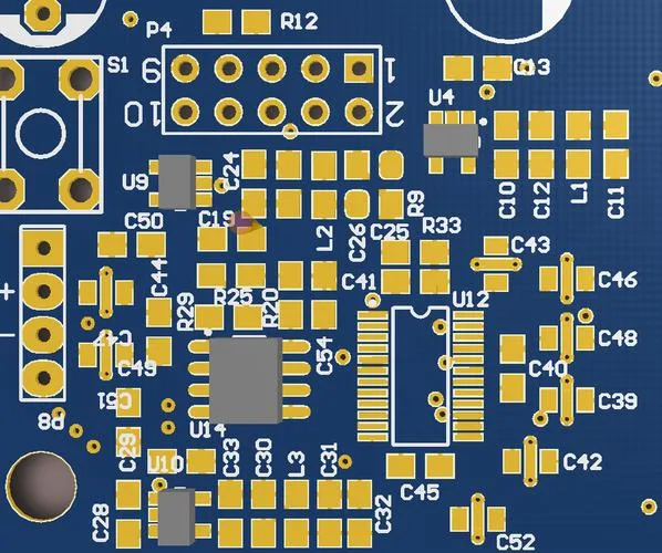
This is one of the most common types, primarily used to mark component locations and designations (e.g., “R1,” “C3,” “D2”) to facilitate subsequent PCB assembly, maintenance, and testing. Advantages include rapid component location, improved maintenance efficiency, and enhanced long-term readability.
Identification Silkscreen
In customized PCB production, identification silkscreen builds customer trust in the product. It includes company logos, product numbers, production dates, and is typically placed on board edges or blank areas. Its functions encompass brand promotion, product traceability, and compliance certification (e.g., RoHS, CE marking).
Functional Labeling Silkscreen
This type of silkscreen appears on PCBs with user interfaces or controls, labeling functional descriptions for ports, switches, or test points (e.g., “TX/RX,” “Power Input”) to reduce operational errors.
3. Why Use Silkscreen on PCBs?
PCB silkscreen enhances efficiency during assembly and testing phases while significantly reducing troubleshooting time. There are numerous benefits to using silkscreen on PCBs.
1) Guiding Component Placement
Position Markings: Silkscreen uses text and symbols to mark component placement locations. This is particularly crucial for complex boards (e.g., computer motherboards with thousands of components), precisely guiding assemblers in installing critical parts like CPUs and memory.
Polarity Indication: For polarized components (e.g., diodes, electrolytic capacitors), silkscreen prevents damage or circuit failures caused by reverse installation through clear positive/negative polarity symbols.
2) Controlling Production and Quality
Test Point Marking: PCB silkscreen clearly identifies test point locations, improving efficiency in detecting open circuits and short circuits.
Version Traceability: PCB silkscreen information like production batches and version numbers facilitates post-production quality tracing and after-sales service.
3) Ensuring Process and Performance
Solder Mask Protection: Screen-printed solder mask ink shields copper foil from corrosion and enhances PCB durability.
Fine Line Fabrication: Modern silkscreen technology enables line widths as low as 12μm, meeting high-density PCB requirements.
4) Supporting User Maintenance
Operational Guidance: Silkscreen provides component part numbers, polarity indicators, and other markings, reducing PCB assembly error rates.
Fault Diagnosis: During repairs, PCB silkscreen allows rapid identification of faulty components, shortening troubleshooting time.
4. Different PCB screen printing technologies and their advantages and disadvantages
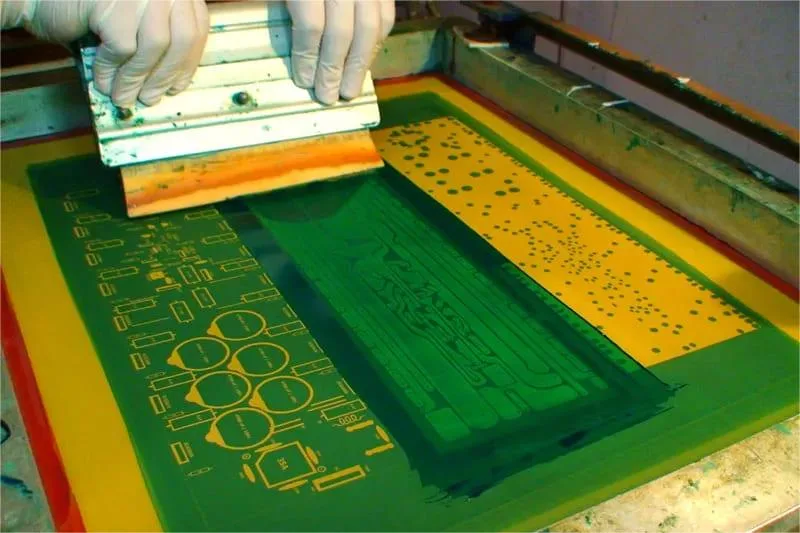
1) Traditional Screen Printing
Manual screen printing is a traditional and relatively economical printing method. This process uses epoxy resin ink, which is applied to the laminate and dried to create the printed pattern on the board.
This screen printing method is straightforward and low-cost, but it also has drawbacks, such as requiring larger spacing between pads and longer stencil drying times. Traditional screen printing is a viable option when budgets are tight and board spacing is not a critical concern.
2) Liquid Photo Imaging (LPI)
Liquid photo imaging closely resembles the process of applying solder mask. In this method, a liquid photo-imageable epoxy resin is coated onto the laminate and exposed to ultraviolet light. Following exposure, the circuit board undergoes development and curing. This process achieves significantly greater precision than manual screen printing.
3) Direct Legend Printing (DLP)
DLP is the most accurate yet costliest of these three screen printing production methods.
In this process, an inkjet projector is used with acrylic ink, which is applied directly from CAD data onto the bare PCB. The ink cures under UV light during printing. Note that acrylic ink will not cure on boards with a silver finish.
Direct Legend Printing utilizes acrylic ink to save drying time. This method offers the highest accuracy and optimal time efficiency, accommodating extremely low text heights. However, text below 0.02 inches is not recommended as it becomes illegible.
| Printing Method | Precision | Cost | Best For |
| Traditional Screen Printing | Low | Low 4 | Budget-friendly, simple boards 5 |
| Liquid Photo Imaging (LPI) | High 6 | Medium | High-density PCBs 7 |
| Direct Legend Printing (DLP) | Highest 88
+1 |
High 9 | Complex, high-accuracy designs 10 |
5. PCB Silkscreen Printing Process: Step-by-Step
PCB silkscreen printing operations can be divided into three stages: silkscreen making, printing, and post-processing. The specific steps are as follows:
1) Silkscreen Making Process
Screen Preparation
Clean the frame and apply base emulsion. After drying, stretch the mesh (maintain tension within standard range; reduce tension for film substrates). Adjust air pressure using a pneumatic stretching machine to ensure uniform tension before applying emulsion to fix the mesh.
Photoresist Coating
Prepare photoresist under yellow light (dissolve photosensitizer with distilled water; avoid metal tools). After settling to eliminate bubbles, coat both sides of the screen twice. Drying temperature must remain below 35°C.
Exposure and Development
Align the film pattern side with the screen for exposure. Immerse in water for 1-2 minutes, then rinse and develop. After air-drying, repair pinholes and perform a second exposure for 10 minutes.
2) Silkscreen Printing Process
Screen Mounting and Ink Preparation
Secure the screen onto the printing press. Prepare the ink (measure viscosity using a Zahn cup and adjust thinner according to process requirements).
Registration Printing
Apply squeegee at a 45°-60° angle. Set pressure to ensure complete ink removal from the screen without residue. Maintain a 30°-45° angle for the ink return blade to guarantee uniform ink coverage. (After applying the screen-printed layer, cure the ink to ensure proper adhesion to the PCB substrate.)
3) Post-Processing Process
Edge Sealing and Inspection
Apply edge sealing agent to all four sides of the screen’s reverse side. Inspect registration accuracy and color fidelity. Verify the printed layer is fully functional and all required markings/symbols are present. Errors or omissions in silkscreen printing may cause PCB assembly failures.
Common Issues and Solutions
Uneven Ink Layers: Adjust screen tension (within ±1N/cm) or squeegee hardness (use a hard squeegee for fine patterns, a soft squeegee for thick ink layers).
Missing Prints: Regularly clean the screen with a lint roller to prevent ink drying and clogging the mesh.
6. PCB Silkscreen Design Considerations
Silkscreen printing must adhere to certain design specifications to enhance the quality of PCB component identification, assembly, and testing.
1) Basic Specification Requirements
Line Width and Spacing
Silkscreen line width must be ≥4 mil (recommended ≥5 mil) to prevent blurring or breakage due to excessive thinness.
Maintain ≥6 mil spacing between silkscreen and pads to avoid pad coverage causing soldering defects.
Minimum spacing between silkscreen elements is 6 mil; overlapping sections must remain distinguishable.
Character Size and Orientation
The height-to-width ratio for characters should be ≥6:1. Common font sizes are 4/25mil (high density), 5/30mil (standard), and 6/45mil (spacious).
Character strings should be arranged following a left-to-right or bottom-to-top reading direction to avoid multi-directional confusion.
2) Layout and Functional Design
Part Numbering and Polarity Markings
Part numbers must correspond one-to-one with components, without inversion or sequence errors; lead markings may be used in high-density areas.
Polarity markings (e.g., “+/-” for electrolytic capacitors, “1” pin for chips) must be clearly visible and unobstructed.
Special Package Handling
Silkscreen dimensions for BGAs, QFNs, and similar packages must precisely match the chip to facilitate soldering alignment.
Screw specifications and quantities should be marked near mounting holes to aid installation positioning.
3) Signal Integrity Considerations
Avoid Covering Critical Areas
Silkscreen must not cover pads, test points, mark points, or high-speed signal traces (e.g., clock lines) to prevent soldering or signal quality issues.
Vias should not be placed on silkscreen to prevent character blurring and misidentification.
High-Speed Trace Protection
Silkscreen must not overlay microstrip line areas on top/bottom layers to prevent impedance variation due to dielectric inhomogeneity.
4) Additional Detail Optimization
Dense Pin Areas: Label pin numbers (e.g., on chips, connectors) to reduce debugging complexity.
Functional Identification: Mark user-interaction components (buttons, indicators) with functional descriptions to prevent ambiguity.
Ambiguity Elimination: Use arrows to indicate signal flow direction on interfaces like RS232 to avoid wiring confusion.
7. Common Issues and Design Recommendations for PCB Silkscreen Polarity Markings
PCB silkscreen polarity markings are a critical aspect of circuit board design, but several problems frequently arise in practical applications.
7.1 Common Issues with Polarity Markings
1) Inconsistent Marking Symbols
Some designs use “+/-” or diode triangle symbols, but differing interpretations of dots and line lengths among designers can lead to polarity misjudgment. For instance, dots may be mistaken for either positive or negative terminals, while subtle variations in line lengths are difficult to discern visually.
When through-hole components rely solely on square pads to indicate polarity, the lack of clear standards can cause confusion with PIN1 markings.
2) Missing or Obstructed Markings
Polarized components (e.g., electrolytic capacitors, diodes) lacking polarity silkscreen markings force reliance on component outline identification, significantly increasing PCB soldering and repair complexity.
Silkscreen markings obscured by pads or components render polarity information invisible.
3) Defective Silkscreen
Silkscreen defects like blurred printing, broken lines, or rough edges may result from improper ink viscosity, mismatched screen mesh count, or PCB surface contamination. For instance, printing defects frequently occur when character sizes are too small (<0.8mm).
7.2 Polarity Marking Design Recommendations
Standardizing PCB silkscreen markings and optimizing processes can significantly reduce the risk of polarity errors.
1) Standardizing Marking Symbols
Prioritize “+/-” or internationally recognized symbols (e.g., color-band markings for electrolytic capacitors), avoiding reliance on single dots or varying line lengths.
For surface-mount components, combine body color bands (e.g., gray stripes on diodes) with dual screen-printed markings.
2) Optimizating Layout and Process
Maintain ≥0.4mm spacing between silkscreen and pads to prevent coverage or contamination.
Select 300-400 mesh screens for small characters (0.8-1.0mm) and control ink viscosity between 25,000-30,000 cP to minimize defects.
3) Enhancing Readability
Standardize silkscreen orientation (e.g., left-to-right arrangement) to prevent characters from being obscured by components.
For high-density boards, selectively mark critical polarity information to reduce redundancy.
7.3 Key Points for Component Polarity Identification
Electrolytic Capacitors: For through-hole types, the negative terminal is marked with a long lead and a wide color band (printed with “-”). For surface-mount types, the negative terminal corresponds to the top black stripe.
Diodes: SMD types mark the cathode with a colored band or horizontal line; through-hole types indicate the cathode with a color ring or notch.
LEDs: The longer lead is the anode; SMD types indicate the cathode with a triangular green solder mask.
8. PCB Silkscreen FAQs
A PCB silkscreen helps manufacturers and designers to identify components quickly. The silkscreen ink is a non-conductive epoxy ink and is highly formulated. Although silkscreens are available in a variety of colours, the three most common colours used in the PCB manufacturing industry are black, white and yellow.
Silkscreen is crucial for helping manufacturers and designers to easily identify components on a PCB by annotating them.
The process of silk screening involves pushing ink through a stenciled mesh screen in order to transfer a design onto a surface. A squeegee is used to force the ink through the open areas of the stencil while the stencil blocks the ink from passing through the other areas.
Gently scrubbing the silkscreen area with a soft-bristled brush or abrasive pad, such as an old toothbrush, can help to remove the ink. This method may be effective for thin layers of PCB silkscreen or when the ink has started to degrade.
For standard silkscreen printing, use the largest font size and line width possible, provided it is no smaller than 50 mil for the font and 7 mil for the line. LPI can go down to 4 mil line widths, while direct printing can go down to 3.
Manual screen printing is a process in which a stencil is used to apply an ink or paste onto a PCB. The stencil has a pattern that is created by a mask which is placed on the stencil. The ink or paste is then squeezed onto the stencil and through the mask, onto the PCB.
To ensure legibility without overcrowding your board, stick to a minimum font height of 0.040 inches (1.016 mm) and a stroke width of 0.006 inches (0.152 mm).
The silkscreen ink is a specially non-conductive formulated epoxy. It comes in various colors, the most common in the industry are black and white.
A silkscreen on a PCB is typically used to display the following information: It shows where the parts are located using reference designators. It helps identify test points. It offers identification numbers unique to each board.
PCB silkscreen is a layer of characters, labels, and symbols that is printed onto the surface of the board.
9. Summary
In the field of circuit board design and manufacturing, PCB silkscreen serves as a critical element on the board surface, playing an indispensable role. It provides engineers, production personnel, and subsequent maintenance technicians with vital information such as component part numbers, locations, and mounting orientations, acting as a core element ensuring the readability and usability of the printed circuit board.
Table of Contents
- 1. Che cosa è la serigrafia PCB? (Definizione e funzioni)
- 2. Quali sono i tipi più comuni di serigrafia su PCB?
- 3. Perché utilizzare la serigrafia sui PCB?
- 4. Diverse tecnologie di serigrafia PCB e i loro vantaggi e svantaggi
- 5. Processo di stampa serigrafica su PCB: passo dopo passo
- 6. Considerazioni sulla progettazione della serigrafia PCB
- 7. Problemi comuni e raccomandazioni di progettazione per le marcature di polarità serigrafiche dei PCB
- 8. Domande frequenti sulla serigrafia PCB
- 9. Riassunto

Get Your PCB Quote!


