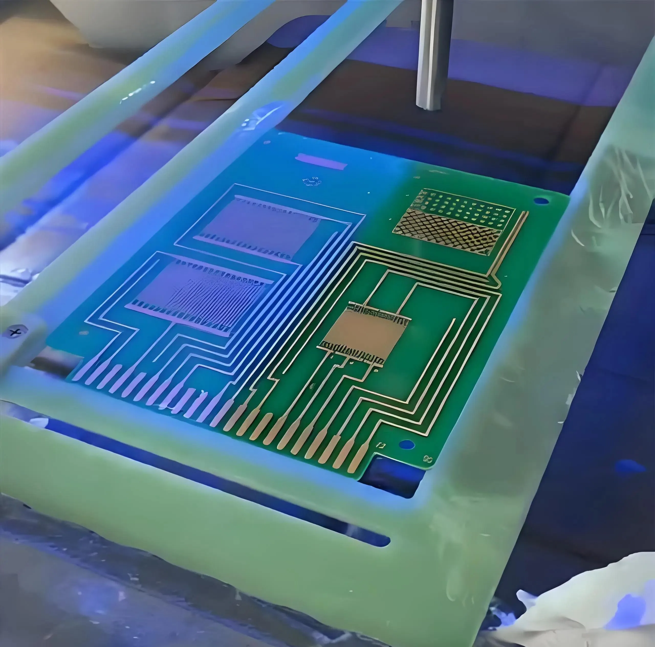
Optimizing PCB Thickness for Signal Integrity & EMI
Three seemingly insignificant parameters—PCB thickness, layers, and tolerance—actually have a critical impact on printed circuit board performance.
Get Your PCB Quote!
Table of Contents
- 1. ПХБ-ийн зузаан гэж юу вэ?
- 2. ПХБ хавтангийн зузаан хүлцлийн стандартууд
- 3. ПХБ-ийн зузааныг сонгохдоо анхаарах ерөнхий хүчин зүйлүүд
- 4. Өөр өөр давхаргад зориулсан ПХБ хавтангийн зузааныг сонгох
- 5. Тохиромжтой ПХБ-ийн зузаан, давхарга, хүлцлийг хэрхэн сонгох вэ?
- 6. ПХБ-ийн зузаантай холбоотой түгээмэл асуултууд
- 7. Дүгнэлт
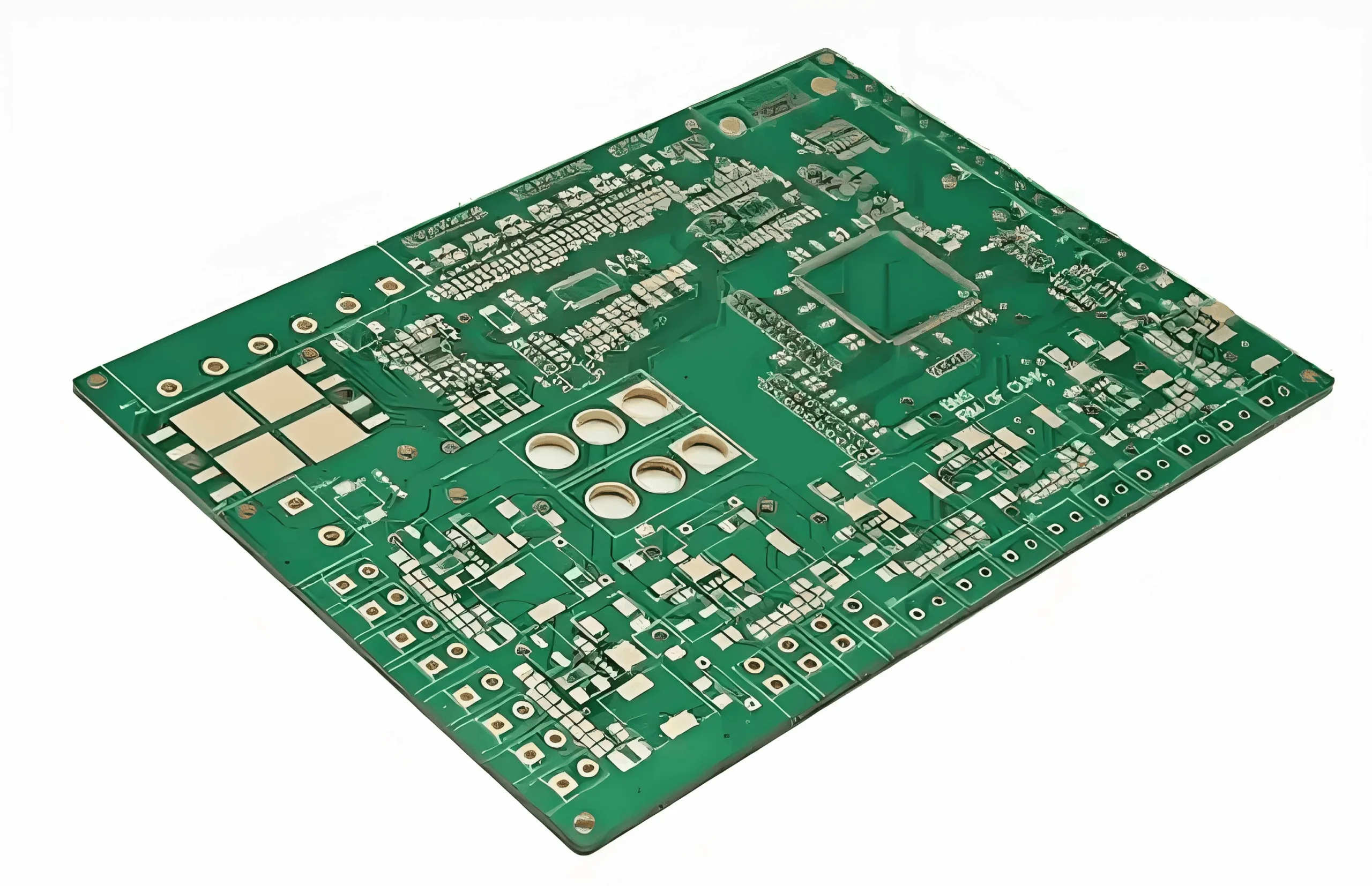
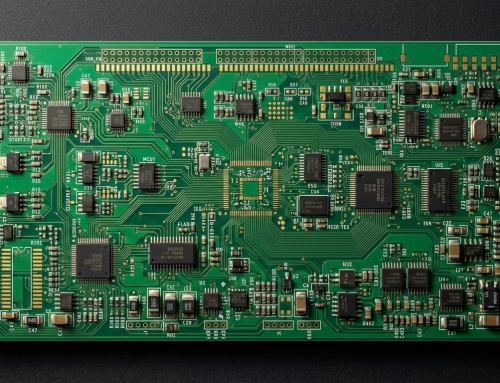
In today’s era of rapid technological advancement, the importance of PCBs (printed circuit boards) as core components in electronic devices is self-evident. They act as bridges connecting various electronic components, ensuring the smooth transmission of electrical currents and signals. However, do you know? There are three things that are important for how well a circuit board works. These are PCB thickness, layer and tolerance. Today, we’re going to take a look at the different thicknesses, layers and standards for PCB production, and how these small details affect the quality of the circuit board.
1. What is PCB Thickness?
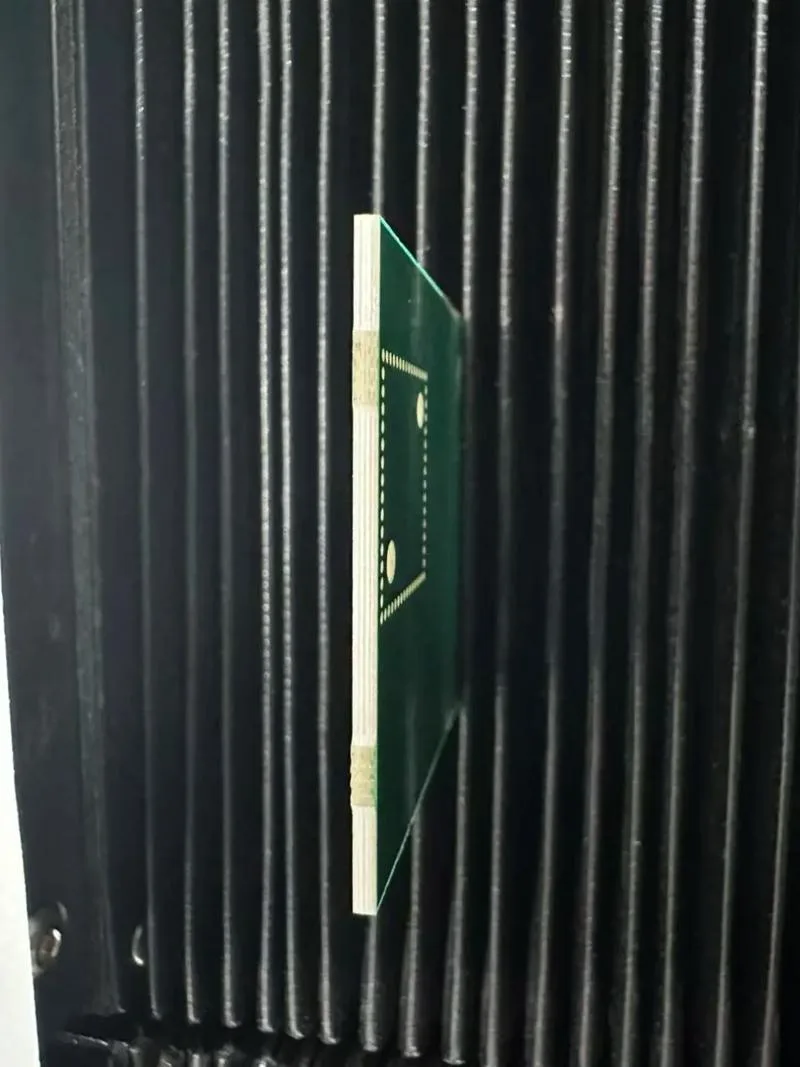
When you hear “PCB thickness,” you might first picture those thin, brittle circuit boards. But in reality, PCB thickness comes in various specifications. The standard thickness is 1.6 millimetres, and circuit boards of this thickness are used a lot in electronic products like computer motherboards and home appliances. It is strong enough to hold things together while also meeting the wiring needs of most electronic components.
However, as electronic devices get smaller and lighter, ultra-thin PCBs are becoming more popular. These circuit boards, which range from 0.2 to 0.8 millimeters in thickness, are used in many small electronic products, such as smartphones and smart wearables. This is because they are lightweight, compact and have a high wiring density. Imagine if your phone were stripped of this thin layer of circuitry—could it still function properly? The answer is clearly no.
Of course, in addition to ultra-thin boards, there are also thick PCB boards. These circuit boards typically range in thickness from 2.4 mm to 3.2 mm. They are used in loads that need to be strong and rigid, like industrial equipment, cars, aeroplanes, and military equipment. In these areas, circuit boards must be stable and reliable, and thick PCB boards are the best choice to meet these needs.
2. Standards of PCB Board Thickness Tolerance
Having covered board thickness, let’s now discuss tolerances. Simply put, tolerance refers to the permissible deviation between actual and theoretical dimensions. For PCBs, the size of the tolerance range directly impacts the quality and performance of the circuit board.
For PCBs that are less than 1 millimetre thick, the coarse tolerance is usually ±10% of the board thickness, and the fine tolerance may be even smaller. This means that for a PCB that is 0.5 millimetres thick, the actual thickness could be between 0.45 and 0.55 millimetres (coarse tolerance), and under fine tolerance control, this fluctuation range may be reduced even further.
For PCBs with a thickness of 1 mm, the tolerance range is typically ±0.08 mm (though some sources cite ±0.1 mm). While this tolerance range may seem minimal, it is critically important in practical applications. This is because the accuracy of the circuit board directly affects how well electronic components can be put together and soldered. This then affects how well the electronic product works and how reliable it is.
When the PCB thickness exceeds 1 millimeter, the tolerance range may increase accordingly. For example, PCB boards with thicknesses of 2 millimeters, 2.4 millimeters, and 3.2 millimeters may have tolerance ranges of ±0.23 millimeters, ±0.25 millimeters, and ±0.30 millimeters, respectively. Although these tolerance ranges are larger than those for thinner boards, they still require strict control to ensure the quality and performance of the circuit boards.
3. General Factors to Consider When Selecting PCB Thickness
When selecting the appropriate thickness for PCBs with varying numbers of layers, multiple factors must be comprehensively evaluated, including signal integrity, mechanical strength, thermal dissipation performance, circuit complexity, and manufacturing costs.
1) Electrical Performance
The electrical performance of a circuit board is one of its most fundamental and critical characteristics. If the PCB is thicker, the signal may take longer to transmit and may become weaker, which can affect the signal integrity. This effect is particularly pronounced in high-speed or high-frequency applications. Therefore, when making high-speed circuit boards, it is very important to strictly control the thickness of the boards and the limits of this thickness. This is essential to make sure that signals do not go off at the wrong time and that they stay stable.
Simultaneously, if the board is too thick, the spacing on the PCB might be uneven, which can affect its electrical performance. For example, if the spacing is too large, it can cause problems like crosstalk and reflections during signal transmission. On the other hand, if the spacing is too small, it can lead to faults such as short circuits or breakdowns.
2) Mechanical Properties
The strength, durability, flexibility, and how well the boards can be routed are the most important mechanical properties of printed circuit boards. Making the PCB thicker makes it stronger and more durable, meaning it can withstand more stress and impact. However, if the board is too thick, it may not be as strong and stable as it should be.
Thinner PCBs are also more flexible and can fit more cables, making them better for devices that need to fit a lot of cables or are very small. Yet, excessive thickness tolerances may compromise flexibility and complicate routing. Therefore, it is very important to strictly control the thickness and range of board thickness when designing and making miniaturised circuit boards. This makes sure that they work well mechanically and that the routing is of a high quality.
3) Thermal Management Performance
As electronic components continue to shrink and integrate, heat density on circuit boards increases significantly. Consequently, thermal management performance has become a critical consideration in PCB design. Thicker PCBs tend to have better heat dissipation because they have more thermal mass and thermal conductivity. This means they can handle heat better. However, excessive PCB thickness tolerances may compromise thermal management stability. For instance, inconsistent thickness in certain areas of the board can lead to uneven heat distribution, potentially affecting the board’s reliability and lifespan.
4) Manufacturing Costs
Finally, let’s discuss manufacturing costs. Thicker boards are better at withstanding pressure and heat, but they also cost more. Additionally, controlling tolerance ranges impacts manufacturing expenses. If the range of acceptable sizes is very small, it will be hard to make the product, which will mean higher costs. So, when choosing PCB thickness and tolerances, it’s important to balance performance needs with cost-effectiveness. This means making sure that the circuit board is good enough and works well, and that it doesn’t cost too much to make.
4. PCB Board Thickness Selection for Different Layers
4.1 2-4 Layer PCB Board
1) PCB Thickness Selection: Common thicknesses include 0.8mm, 1.0mm, 1.2mm, 1.6mm, and 2.0mm. Among these, 1.6 mm is a good choice for most applications because it is stable and reliable.
2) Influencing Factors
Signal Transmission: With fewer layers, signal transmission is relatively straightforward. These thicknesses generally ensure signal integrity.
Mechanical Strength: For simple circuit layouts, these thicknesses provide sufficient mechanical support.
Manufacturing Cost: Thicker boards may incur slightly higher costs. However, for this layer range, the common thicknesses listed above are easy to make, so there is not much difference in cost.
4.2 6 Layers PCB Board
1) PCB Thickness Selection: Inner layers 1/2 oz – 1 oz, outer layers 1 oz – 2 oz (oz denotes copper foil thickness). The board is usually about 1.6 mm thick, but this can be changed a bit based on what the customer needs.
2) Influencing Factors
Signal Integrity: As layer count increases, signal transmission complexity slightly rises. Appropriate copper thickness helps maintain signal quality.
Mechanical Strength: Meets mechanical support requirements for moderately complex circuits.
Thermal Performance: By carefully choosing how thick the inner and outer layers of copper are, we can meet some of the thermal needs.
4.3 8 Layers PCB Board
1) PCB Thickness Selection
Inner layers: For inner layers 1–4, a thickness of 0.1mm is generally recommended.
Outer layers: For outer layers 1–4, a thickness of 0.15mm is recommended. This laminate structure balances signal integrity, mechanical strength, and thermal dissipation requirements. However, specific project needs may vary and require adjustments based on actual conditions.
2) Influencing Factors
Signal Integrity: The 8-layer board has a special design where the inner layers are slightly thicker than the outer layers. This makes the signal stronger.
Mechanical Strength: This thickness configuration enables the 8-layer board to withstand various forces and pressures during assembly, ensuring overall board stability.
Thermal Performance: The material is made up of thinner inner layers and thicker outer layers. This helps to spread heat more effectively, which makes it suitable for use in high-power electronics such as amplifiers and inverters.
4.4 14-16 Layer PCB Board
1) PCB Thickness Selection: Inner layers 1/2 oz – 1 oz, outer layers 1 oz – 2 oz. Overall board thickness is determined by specific design and manufacturing requirements. Typically, thickness is made as thin as possible to reduce costs and fit in smaller spaces, without affecting how well it works.
2) Influencing Factors
Signal Integrity: Making sure the signal is strong enough becomes more difficult as there are more layers. So it is very important to choose the right thickness of copper.
Mechanical Strength: It is important to consider how stable the mechanical parts are in multilayer structures. This helps to prevent problems like warping, which can be caused by the thickness of the boards being wrong.
Manufacturing Cost: Increased layer counts elevate manufacturing complexity and expense. Selecting appropriate board thickness aids in cost optimization.
5. How to Select Appropriate PCB Thickness, Layers, and Tolerance?
5.1 PCB Thickness Selection
The thickness of PCB boards should be chosen based on how they will be used and how strong they need to be. Common standard thicknesses include 0.4mm, 0.6mm, 0.8mm, 1.0mm, 1.2mm, 1.6mm (most commonly used), and 2.0mm.
1) Thin boards (0.4mm–0.8mm): Suitable for small, low-power devices (e.g., smart wearables).
2) Standard boards (1.6mm): It balances how strong it is and how it works, and is used a lot in computer motherboards and home appliances.
3) Thick boards (≥2.0mm): Employed in high-power or high-reliability scenarios (e.g., industrial equipment, automotive electronics).
5.2 Design Principles of PCB Layers
The number of PCB layers depends on how complex the signal is, how well the boards work with other electronic equipment, and how much it costs.
1) Single/double-sided boards: Simple circuits, low cost.
2) Multilayer boards (4 layers and above): The design must be symmetrical. The inner layer of copper must be at least 0.5 oz thick, and the dielectric must be at least 0.1 mm thick. This is to stop breakdown. Additional layers are required for high-density signals or power planes.
5.3 Tolerance Control for PCB Thickness
Tolerances directly impact assembly accuracy and must be determined based on plate thickness and production processes:
Plate Thickness Tolerance:
1)<1mm: ±0.1mm (e.g., 0.8mm thickness PCB is actually 0.7–0.9mm thick).
2) ≥1mm: ±10% (e.g., 1.6mm thickness PCB is 1.44–1.76mm thick).
3) Hole Diameter Tolerance: 0.13mm to -0.08mm (e.g., 0.6mm hole may measure 0.52–0.73mm).
4) Outline Tolerance: Rounded edges ±0.2mm, V-cut panel joints ±0.04mm.
5.4 Comprehensive Recommendations
1) Prioritize standard thicknesses (e.g., 1.6mm) to reduce costs.
2) High-power equipment requires thicker boards and increased copper thickness (e.g., 2oz).
3) Precision assemblies demand strict tolerance control; precision tolerance processes are recommended.
6. PCB Thickness FAQs
Standard PCB thickness ranges from 0.2mm to 3.2mm, with common thicknesses including 0.4mm, 0.6mm, 0.8mm, 1.0mm, 1.2mm, 1.6mm, and 2.0mm. Selection depends on application requirements, mechanical strength needs, and electrical performance specifications.
PCB thickness is a critical parameter affecting circuit board performance and reliability.
Thickness directly determines the board’s resistance to bending and impact.
Thicker PCBs (e.g., 1.6mm) offer superior thermal conductivity.
Thickness influences transmission line impedance and signal integrity.
Increased thickness significantly elevates dielectric loss. At 10GHz, the loss (0.8dB/cm) for a 1.6mm board is 33% higher than for a 1.0mm board (0.6dB/cm); at 28GHz, this gap widens to 50%.
Thin boards (1.2-1.6mm) used in high-frequency devices (e.g., routers) reduce signal loop area and lower radiation. Actual measurements show that reducing thickness from 2.0mm to 1.6mm decreased 5GHz band radiation emissions from 54dBμV/m to 46dBμV/m.
Consumer electronics: Prioritize 1.6mm or ultra-thin boards (below 0.8mm) to save space.
Industrial/automotive: Select 2.0-3.2mm thick boards to ensure reliability.
High-frequency/high-speed signals: Optimize thickness by balancing dielectric constant and interlayer capacitance.
Thicker PCBs (e.g., 1.6mm) balance component heat generation with natural convection cooling, preventing device overheating. Thin boards offer weaker thermal management, potentially shortening high-power component lifespans.
7. Summary
PCB thickness, tolerance, and layers selection need to be balanced to make sure the signal works well, it’s strong enough, and it doesn’t cost too much. 2-4 layers commonly use 1.6mm for stability and cost-effectiveness; 6 layers emphasize copper foil ratio optimization for signal performance; 8 layers utilize differentiated laminate control for heat dissipation; 14 layers and above require precision design to prevent warping. Ultimately, you must make decisions based on comprehensive consideration of your application scenario and requirements, while strictly controlling manufacturing processes and tolerance ranges to ensure the quality and performance of the circuit board.
Table of Contents
- 1. ПХБ-ийн зузаан гэж юу вэ?
- 2. ПХБ хавтангийн зузаан хүлцлийн стандартууд
- 3. ПХБ-ийн зузааныг сонгохдоо анхаарах ерөнхий хүчин зүйлүүд
- 4. Өөр өөр давхаргад зориулсан ПХБ хавтангийн зузааныг сонгох
- 5. Тохиромжтой ПХБ-ийн зузаан, давхарга, хүлцлийг хэрхэн сонгох вэ?
- 6. ПХБ-ийн зузаантай холбоотой түгээмэл асуултууд
- 7. Дүгнэлт

Get Your PCB Quote!