PCB Warpage Tolerance & Prevention: Guide for Wave Soldering
This paper discusses the issue of PCB assembly warpage and proposes a series of prevention and flattening methods to minimize its impact on the PCBA process.
Get Your PCB Quote!
During PCB assembly, warpage of the PCB board is a common and challenging issue. It not only hinders the placement of SMT electronic components but may also lead to poor solder joint contact and even damage the substrate during lead trimming. Furthermore, during wave soldering, warped substrates may prevent certain pads from making proper contact with solder, thereby compromising soldering quality. Consequently, for printed circuit board manufacturers, preventing PCB assembly warpage and effectively addressing warped PCB boards are critical priorities.
1. What is PCB Assembly Warpage?
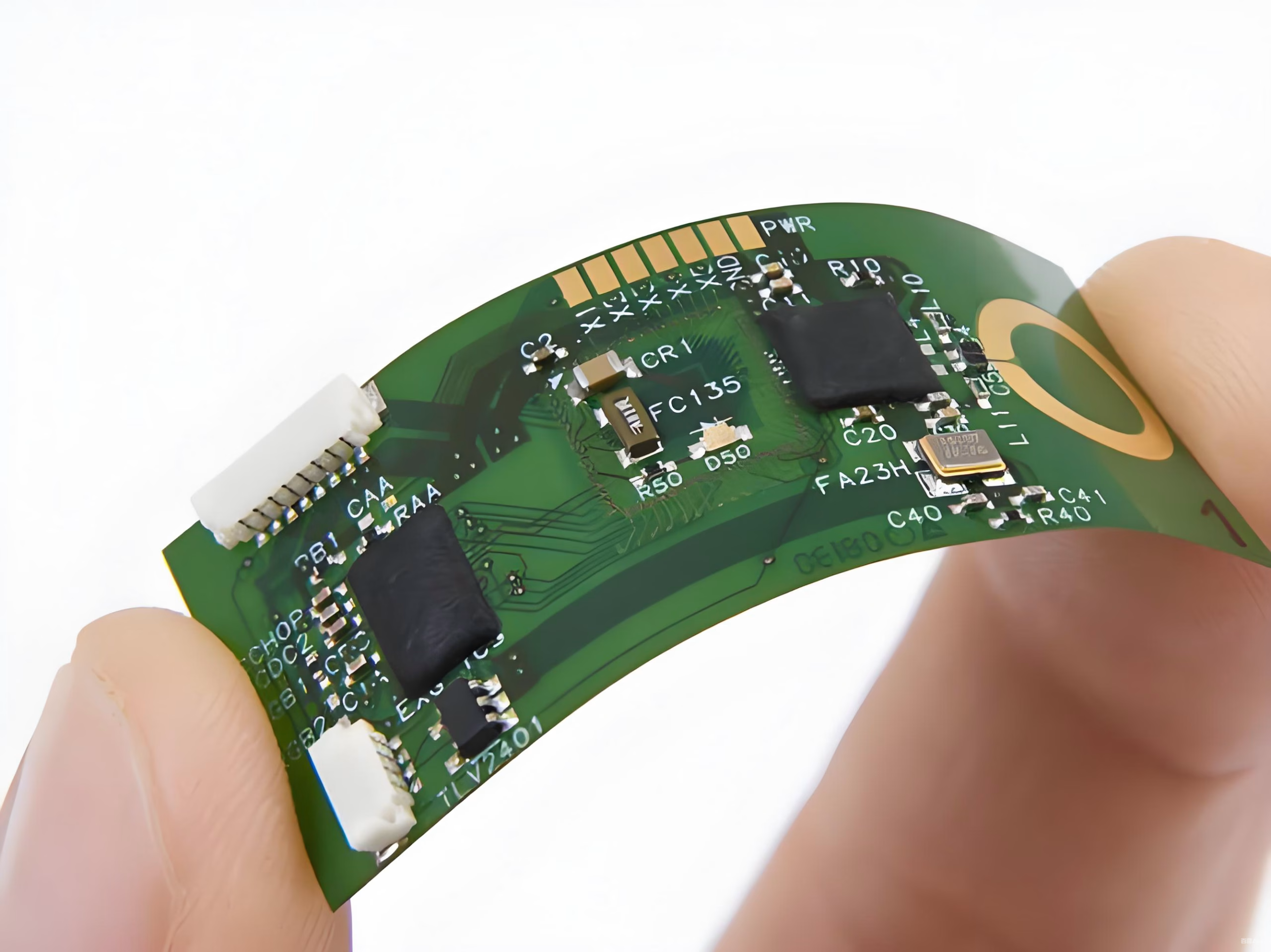
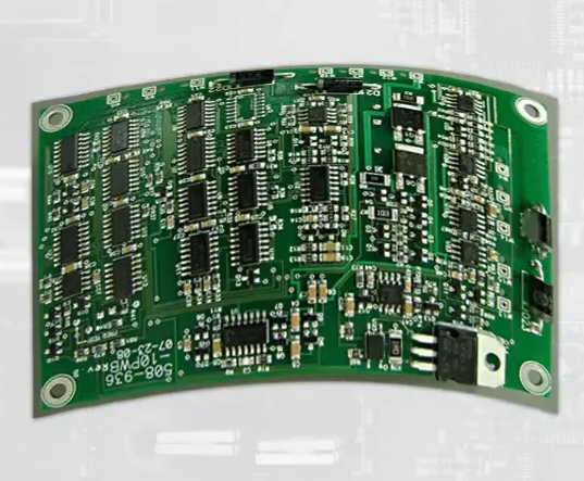
Warpage, as the name suggests, refers to whether a printed circuit board (PCB) is flat and can be perfectly inserted into the board’s holes and surface mount pads. Ideally, when a PCB is placed on a flat reference surface, all parts of it should contact that surface. However, due to various stresses, this is not always the case, and certain parts of the PCB may fail to make contact with the surface. Certain areas of the PCB may bend upward while others bend downward, exhibiting positive and negative curvature respectively. Furthermore, the bending direction may occur along one or both axes of the circuit board, or along one or both diagonals. The board may also experience warping. All these phenomena fall under the category of PCB assembly warpage.
1.1 PCB Warpage Standards
According to IPC standards, the warpage (WD) of PCBs intended for assembly must be less than or equal to 0.75%. This means that when WD exceeds 0.75%, the board should be classified as warped or defective.
In practice, when boards require only through-hole components without surface mounts, lower flatness is acceptable, allowing a WD tolerance of ≤1.5%.
Certain manufacturers pursue stricter standards to meet higher customer demands, with WD tolerances as low as ≤0.5% or even ≤0.3%.
1.2 PCB Warpage Calculation Formula
Warpage typically refers to deformation where the plastic part’s surface fails to conform to the designed shape. Numerous factors influence warpage, necessitating careful attention during production. After all, even minor errors can render an entire circuit board unusable. So, how is PCB warpage calculated?
WD= Single-corner warp height / (PCB diagonal length × 2) × 100%
2. Hazards of PCB Assembly Warpage
During automatic insertion, an uneven PCB can cause positioning errors and even cause the automatic insertion machine to freeze. If the board warps after component soldering, it becomes extremely difficult to neatly cut component leads. Ultimately, this prevents the PCB from fitting into sockets within the chassis or machine, effectively rendering the circuit board unusable. Therefore, encountering PCB assembly warpage is a painful issue for manufacturers.
Production Failures: Misalignment during placement may damage equipment; uneven component leads after soldering prevent installation.
Performance Issues: Signal transmission delays, solder joint cracking, and reduced circuit stability.
Reliability Risks: Poor heat dissipation accelerates component aging; mechanical stress may cause fractures.
Increased Costs: Reduced assembly efficiency, higher defect rates, and elevated repair expenses.
3. Causes of PCB Assembly Warpage
PCB assembly warpage arises from complex factors, stemming either from substrate irregularities or thermal stress, chemical effects, or improper manufacturing processes during production.
1) Material Factors
CTE Mismatch: Significant thermal expansion coefficient (CTE≈17ppm/℃ for copper foil vs. CTE≈50-70ppm/℃ for substrates like FR-4) leads to uneven contraction/expansion during temperature changes.
Moisture Absorption: Resin substrates absorb water, causing thermal expansion and generating stress.
Uneven Copper Distribution: Significant variations in copper layer thickness across the board surface (e.g., large copper-clad areas vs. non-copper areas) result in differing cooling contraction rates.
2) Design Factors
Asymmetric Laminate: Non-symmetrical structures (e.g., 6-layer board using 1-2-2-1 stackup) cause Z-axis stress imbalance.
Copper Balance Disruption: Uneven copper distribution within a single layer, or mismatched copper pattern positioning/density between adjacent layers.
Mechanical Structural Defects: Panel layouts lacking process edges, excessively deep V-cuts, or unfortified areas around connectors/mounting holes.
3) Process Factors
Lamination Process: Uneven pressure/temperature or excessive cooling rates prevent internal stress release.
High-temperature Processes: Abrupt temperature rises/drops in reflow/wave soldering accelerate CTE-induced differential deformation.
Processing Stresses: Residual stresses introduced by drilling, milling, or other machining operations.
4) Environmental Factors
Temperature/Humidity Fluctuations: Storage humidity >60% or thermal shocks (e.g., frequent equipment cycling) accelerate fatigue warpage.
Mechanical Stress: Over-tightened screws during installation, bending, or vibration impacts cause permanent deformation.
5) Other Factors
Excessively Thin Thickness: PCBs <0.8mm thick lack sufficient rigidity and are more prone to warping.
Heavy Component Placement: Localized overloads from large BGAs, heat sinks, etc., cause sagging under prolonged gravitational force.
Additionally, to enhance assembly efficiency, manufacturers typically assemble PCB boards into panels. During panel assembly, guide rails and brackets are used to facilitate panel handling throughout various assembly stages. After assembly is complete, operators remove the brackets and separate the PCB boards through de-panelization. The difference in copper density between the bracket area and the circuit board area also contributes to warpage.
4. How to Prevent PCB Assembly Warpage?
Preventing PCB assembly warpage requires a comprehensive approach that includes process selection, material optimization, and adherence to best design practices.
1) Engineering Design Optimization
Layer Symmetry: Ensure symmetry in the number and thickness of prepreg sheets between layers 1-2 and 5-6 in multilayer boards to prevent warpage caused by uneven material shrinkage.
Circuit Balance: Copper foil area on outer layers A/B should be similar. For significant differences, add grid patterns on the sparser side to balance stress.
Unified Materials: Core boards and prepregs must come from the same supplier to ensure consistent thermal expansion coefficients.
2) Process Control
Pre-baking Dehumidification: Bake at 150°C for 8 hours prior to cutting to eliminate residual moisture and stress within the substrate.
Orientation Management: Distinguish between the warp (curling direction) and weft orientation of prepreg sheets; maintain consistent orientation during lamination.
Post-lamination treatment: Bake at 150°C for 4 hours to release lamination stresses.
3) Material and Structural Selection
High-Tg Laminate: Increase the glass transition temperature to enhance resistance to deformation.
Increase Board Thickness: 1.6mm thickness is less prone to warping than 0.6mm.
Reduce Panel Assembly: Smaller dimensions and fewer panels minimize weight-induced warpage.
4) Production Support Measures
Reflow Trays: Secure PCBs to maintain flatness during reflow soldering, especially for thin boards.
Alternative to V-cut: Use router-cut separation to minimize structural damage.
Cooling Control: Allow natural cooling after hot air leveling to prevent rapid cooling deformation.
5. How to Fix Warped PCBs?
1) Warp Correction During PCB Assembly
During PCB processing, boards with significant warping are identified by roller leveling machines and flattened before proceeding to subsequent steps. Many PCB manufacturers consider this method effective for reducing warp rates in finished boards.
2) Warp Correction for Assembled PCBs
For finished boards with excessive warpage beyond tolerance limits, roller leveling machines are ineffective. Some PCB factories place warped boards in small presses (or similar fixtures) for cold pressing over several to ten hours. Practical experience shows this method yields limited results: first, the leveling effect is minimal; second, flattened boards often spring back (i.e., warpage recurs).
Some PCB manufacturers heat the small press to a specific temperature before applying thermal pressure to flattened PCBs. This yields better results than cold pressing, but excessive pressure can cause component deformation; excessively high temperatures may lead to defects like rosin discoloration. Moreover, both cold and hot pressing require extended periods (ranging from several to over ten hours) to achieve visible results, and the rate of warpage rebound after flattening remains high.
Here, we recommend a bow-shaped mold hot-pressing method. Based on the PCB area requiring flattening, use a simple bow-shaped mold for leveling. There are primarily two operational approaches:
Method 1: Clamp warped PCB boards into a bow-shaped mold and bake them flat in an oven
Position the curved side of the warped PCB board against the mold’s curved surface. Adjust the clamp screws to deform the PCB board in the opposite direction of the warp. Then place the mold with the PCB board into an oven heated to a specific temperature and bake it for a period of time. Under heating conditions, substrate stress gradually relaxes, restoring the deformed PCB to a flat state. However, baking temperature should not be excessively high to prevent rosin discoloration or substrate yellowing. Conversely, temperatures should not be too low, as complete stress relaxation requires significantly longer durations at lower temperatures.
Typically, the substrate’s glass transition temperature serves as the reference baking temperature. This phase transition point allows polymer chains to rearrange, enabling full stress relaxation. The bow-shaped mold offers significant flattening effectiveness with minimal investment, as ovens are readily available in PCB factories. The leveling process is straightforward. For large quantities of warped boards, preparing several bow-shaped molds suffices. You can load them into the oven simultaneously. With fewer molds, drying time is shorter (around several tens of minutes), making the leveling operation highly efficient.
Method 2: Soften the PCB board and press it flat using a bow-shaped mold
For PCB boards with minor warping deformation, place the board to be flattened into an oven preheated to a specific temperature (set based on the substrate’s glass transition temperature). Bake the substrate in the oven for a certain duration, then observe its softening state to determine the appropriate temperature. Generally, higher baking temperatures are required for glass fiber cloth substrates, while paper-based substrates can tolerate lower temperatures. Thicker boards may benefit from slightly higher temperatures, while thinner boards may require slightly lower temperatures.
For rosin-coated PCBs, avoid excessively high baking temperatures. After baking, take several to a dozen boards, clamp them into a bow-shaped mold, adjust the pressure screws, and gently warp the PCBs in the opposite direction. Once cooled and set, remove the mold to obtain flattened PCBs. Bow-mold flattening minimizes warpage; They generally maintain flatness even after wave soldering; the impact on PCB surface appearance is also minimal.
PCB assembly warpage is a persistent headache for PCB manufacturers. It not only reduces yield but also impacts delivery schedules. Employing bow molds for thermal flattening, when the process is properly designed and executed, can effectively flatten warped PCBs and resolve delivery time constraints.
6. Warpage FAQs
PCB assembly warpage is when a Printed Circuit Board (PCB) bends or deforms during manufacturing, especially during processes like soldering.
PCB warpage is a defect where PCB boards become distorted or bent out of its original flat shape. It can happen on bare PCBs and also finished PCBAs.
Material Optimization: Select substrates with high Tg values and low CTE (e.g., FR-4).
Design Improvements: Increase board thickness to 1.6mm or above, ensure balanced copper foil distribution, and avoid V-cut panelization.
Process Control: Ensure lamination alignment, implement controlled cooling after curing, and use forced convection ovens.
Soldering Issues: Causes cold solder joints, short circuits, or component detachment.
Mechanical Risks: Solder joint stress concentration during installation may lead to fractures.
Functional Failure: Severe deformation may prevent device assembly.
Lead-free reflow soldering operates at higher temperatures (up to 260°C). Select high-temperature-resistant substrates (e.g., phenolic-cured FR-4) and optimize temperature profiles.
Marble Test Method: Measure the ratio of the PCB’s central arch height to its diagonal length.
Optical Inspection Method: Use a flatness gauge with precision down to 0.1 mil.
7. Summary
This paper delves into the issue of PCB warpage and proposes a series of prevention and flattening methods to minimize its impact on the PCB assembly process. Every stage from inventory management to manufacturing processes directly or indirectly influences PCB assembly warpage. Implementing proper storage practices, optimized circuit design, precise soldering temperature control, and stress-relief treatments can effectively prevent warpage occurrence. For warped PCBs, the bow-shaped mold hot-press leveling method effectively restores flatness, enhances yield rates, and ensures timely delivery.

Get Your PCB Quote!