Explore the PCB Board Fabrication Process, Raw Materials and Finished Board
Step-by-step guide to PCB fabrication - from FR4 substrate to final testing, covering etching, drilling, soldermask application and quality control.
Get Your PCB Quote!
Table of Contents
- 1. ابدأ بالمادة الأساسية: الركيزة
- 2. نقل التصميم: من الرقمي إلى المادي
- 3. إزالة النحاس الزائد عن طريق النقش
- 4. حفر ثقوب للتوصيلات الكهربائية
- 5. وضع الثقوب - ضمان التوصيل
- 6. كيفية تطبيق قناع اللحام للحماية والوضوح
- 7. أضف ملصقات وعلامات الطباعة الحريرية
- 8. تشطيب السطح: تحضير تركيب المكونات
- 9.الاختبارات الكهربائية: اكتشاف العيوب
- 10. التغليف النهائي والفحص
- 11. ملخص
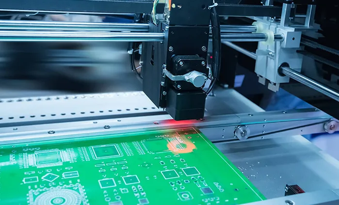
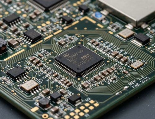
Every Electronic device like smartphone, laptop, medical devices or industrial equipment works with the support of quality PCBs. Have you ever wondered just how these complex boards are created? The PCB board fabrication is a fascinating mix of engineering, precision and innovation. We’ll walk you through the PCB journey, from the raw materials to a fully-functional board that powers your gadgets.
1.Start with the Base Material: Substrate
It all starts with opting the correct base material. Most PCBs use a fiberglass-reinforced epoxy laminate called FR4. The structural core is made of this non-conductive material. This base is coated with copper foil on either one or both sides, depending on if the board is double-sided or single-sided.

The final application of a board will determine the material to be used. You may need specialized substrates for environments with high temperatures or frequencies. A reputable PCB board manufacturer will guide you in the selection of materials based on performance requirements and budget.
2.The Design Transfer: From Digital to Physical
Let’s run your design into the market. A digital blueprint is printed on a film to help define the layout of copper wires.
To remove all contaminants, the copper-clad panel is thoroughly cleaned. The application of a light-sensitive material on the board surface. The board is exposed to the specially prepared film and UV light that transfers the pattern onto it. The photoresist is hardened in the areas that should retain traces, and the copper is protected by the unexposed areas.
3.Remove Copper Excess by Etching

The board is then immersed in a chemical solution, usually ferric chloride (or an alkaline Etchant). The copper is removed, leaving only the photoresist-defined traces and pads.
Now, it’s time to stop any chemical reaction after etching the board. After removing the remaining photoresist, copper paths that will transmit electrical signals are revealed.
The precision of this step can often be the difference between a good PCB fabrication manufacturer and a poor one. This phase is crucial, as any error can result in circuit failure or poor connectivity.
4.Drilling Holes for Electrical Connections

After the traces are in place, holes will be needed for interlayer connections and components. Through-hole components, vias (small copper holes connecting layers on multi-layer PCBs) and inter-layer connections are made using computer-controlled drilling.
This drilling process is extremely accurate. A slight misalignment could cause short circuits or connection failures. This is why manufacturers use high- speed and high- perfection CNC machinery.
5.Placing the Holes – Ensure Conductivity
Electrochemically, after drilling the holes, a thin copper layer is applied. The conductive pathway between the layers is created. This internal connectivity is essential for multi-layer boards to work correctly.
A good plating job is an important quality standard. A reputable PCB board manufacturer follows strict quality control during this phase in order to ensure consistency conductivity and reliability.
6.How to Apply the Solder Mask for Protection and Clarity

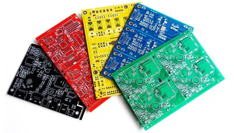
The board is then coated with a mask of solder after the copper circuitry has been completed. The familiar green layer (or, sometimes, red, blue or black) that you see on completed PCBs is this solder mask. Solder masks prevent accidental solder bridges and protect the copper against oxidation and corrosive corrosion.
A solder mask is a layer of liquid that covers the printed circuit board and protects the copper traces from unwanted soldering. The places where components are to be connected to the PCB are left open. Solder mask is hardened using UV light or heat.
7.Add the Silkscreen Labels and Markings

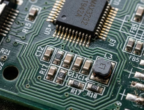
The silkscreen is then printed over the solder mask. This layer contains symbols, labels and other information such as component values or test points. This layer is used by technicians and engineers to assemble test and repair the board.
Silkscreen designs can be used to improve circuit usability, and even help troubleshoot complex ones. Although labels may seem unimportant, they are extremely useful for production and maintenance.
8.Surface Finishing: Preparing Component Mounting

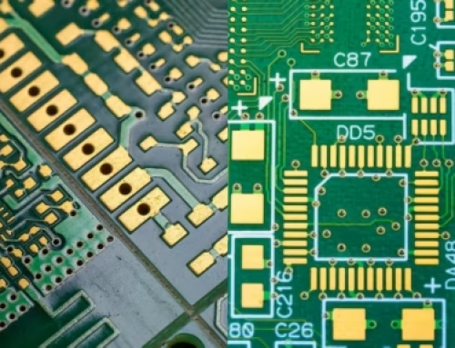
The board should now be structurally and visually complete. Next, the copper pads exposed need to have a solderable and defensive finish applied. Finishes include HASL, ENIG (Electroless Nitino Immersion Gold) and OSP.
Each finish has advantages. ENIG, for example, is a finish that offers excellent surface planarity. It’s also ideal for components with fine pitches. The right PCB manufacturer will select a finish aligned with the assembly process and performance requirements of their customers.
9.Electrical Testing: Finding Defects
Before the board is assembled or shipped, it is tested several times for electrical defects. This includes continuity (to ensure that all of the connections have been made) and isolation.
The latest systems can test thousands connections in just seconds. A defect detected at this stage could save money, time and even prevent failures in the future.
10.Final Packaging and Inspection
Visual inspection and final cleaning are the last steps in the PCB board fabrication. Automated Optical Inspection systems (AOI) scan the board to detect surface defects such as scratches, misalignments or excess solder. Some high-end applications require X-rays to check that internal layers are aligned.
After the board has passed all quality tests, it will be carefully packaged in order to avoid damage during transport. The boards can be delivered as individual units, arrays or panels depending on the customer’s needs.

11. Summary
PCB fabrication involves a multi-step procedure that blends perfection, technology and experience. An experienced PCB maker comes with an extensive design options that’s why it’s vital to choose them.
It is vital to opt the professional PCB fabrication manufacturer with the advanced project management strategy. If you’re looking for a manufacturer that is committed to quality, they will make sure your design becomes an effective and durable board. industrial equipment and medical devices might have board in the fabrication process.
Think about the PCB, a silent but important component, next time you use your smart phone or appliance. The amazing journey from raw materials to finished boards. So, this post might be your ideal guide to know the PCB’s raw materials and the overall board fabrication.
Table of Contents
- 1. ابدأ بالمادة الأساسية: الركيزة
- 2. نقل التصميم: من الرقمي إلى المادي
- 3. إزالة النحاس الزائد عن طريق النقش
- 4. حفر ثقوب للتوصيلات الكهربائية
- 5. وضع الثقوب - ضمان التوصيل
- 6. كيفية تطبيق قناع اللحام للحماية والوضوح
- 7. أضف ملصقات وعلامات الطباعة الحريرية
- 8. تشطيب السطح: تحضير تركيب المكونات
- 9.الاختبارات الكهربائية: اكتشاف العيوب
- 10. التغليف النهائي والفحص
- 11. ملخص
Get Your PCB Quote!

