DIP vs. SMD: How to Choose the Right Component Package
From early DIP to today's SMD package, each innovation of component package has propelled electronic devices toward becoming smaller, faster, and more powerful.
Get Your PCB Quote!
Table of Contents
- 1. component Package နည်းပညာ ျခံဳငံုသံုးသပ္မႈ
- 2. ရိုးရာအထုပ်e: DIP (Dual In-line Package)
- 3. SMD Package- Surface Mount Technology (SMT) ထွန်းကားလာခြင်း
- 4. နည်းပညာဆိုင်ရာ နှိုင်းယှဉ်မှု နှင့် ရွေးချယ်ရေး အကြံပြုချက်များ Component Package ၏
- 5. အနာဂတ်ရေစီးကြောင်းများ DIP နှင့် SMD Package များ
- 6. အစိတ်အပိုင်းအစုံအလင် FAQs
- 7. အကျဉ်းချုပ်
Every miniaturization and performance leap in electronic devices begins with the symbiotic evolution of component package technology and PCB manufacturing processes. The advent of Surface Mount Technology (SMT) revolutionized how electronic components are mounted. From early DIP package to today’s SMD package, each innovation in packaging technology has propelled electronic devices toward becoming smaller, faster, and more powerful. Driven by smartphones, IoT devices, and AI hardware, packaging forms have evolved from simple two-pin structures into highly integrated three-dimensional interconnect systems.
1. Component Package Technology Overview
Chip packaging, simply put, involves mounting the bare die produced by the foundry onto a substrate that serves as a carrier. The pins are then brought out and secured into a unified package. This structure protects the chip, acting as its outer shell. It not only secures and seals the chip but also enhances its electrical and thermal performance. Therefore, component package is critically important for CPUs and other LSI integrated circuits.
Package types can be broadly categorized into two main categories: DIP (Dual In-line Package) and SMD (Surface Mount Device).
Structurally, component package evolved from the earliest transistor TO (Twin Outline) packages (such as TO-89 and TO-92) to dual in-line packages. Subsequently, PHILIPS developed the SOP (Small Outline Package), which later branched into S0J (Small Outline Package with J-type leads), TSOP (Thin Small Outline Package), VSOP (Very Small Outline Package), SSOP (Shrink Small Outline Package), TSSOP (Thin Shrink Small Outline Package), SOT (Small Outline Transistor), and SOIC (Small Outline Integrated Circuit).
Regarding material substrates of package, these include metal, ceramic, and plastic. Metal packaging remains prevalent in circuits requiring high-strength operating conditions, such as military and aerospace applications.
2. Traditional Package: DIP (Dual In-line Package)
DIP is an integrated circuit packaging technology invented by Bryant Buck Rogers in 1964. The first device featured a 14-pin design.
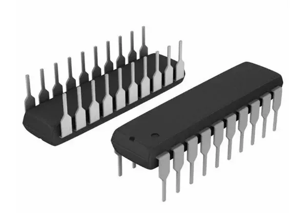
2.1 What are the Core Characteristics of DIP Package?
1) Package Structure
Appearance: Rectangular package body with symmetrically arranged vertical leads on both sides. Standard lead pitch is 0.1 inches (2.54 mm), with common row pitches of 0.3 inches or 0.6 inches.
Pins: Typically 6–64 pins (designated as DIP n, e.g., DIP14 denotes a 14-pin model), generally not exceeding 100 pins.
Material: Manufactured from plastic or ceramic; ceramic is predominantly used in high-reliability equipment.
2) Technical Features
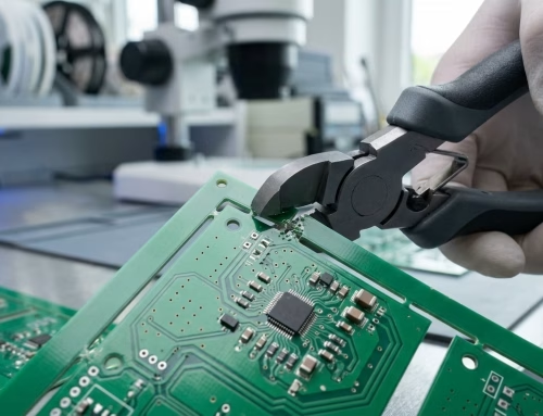
Mounting Method: Through-hole soldering involves using pins to attach components to a PCB. These components are either mounted using through-hole technology or inserted into DIP sockets. Through-hole soldering is compatible with wave soldering processes and manual assembly.
Compatibility: Pin spacing aligns with breadboard layouts, facilitating circuit prototyping, educational experiments, and maintenance testing.
Limitations: Bulky form factor, low density, typically ≤100 pins, prone to damage, gradually replaced by SMD.
3) Applications and Evolution
Historical Significance: DIP package dominated the microelectronics industry during the 1970s-1980s, widely used in microprocessors, memory chips, and similar components. Examples include early CPUs (e.g., 8086), memory chips, and legacy BIOS chips.
Current Status: DIP has been largely replaced by Surface Mount Device (SMD) due to SMD’s advantages in space density and production efficiency. However, DIP remains in use for industrial equipment, low-end electronics, and prototyping scenarios.
2.2 How to Properly Install DIP-Packaged Chips?
1) Pin Alignment
Align the chip’s notch or markings with the PCB socket’s notch, ensuring both rows of pins are fully inserted into the through-holes. The standard DIP pin pitch is 2.54mm, which must match the PCB design.
2) Vertical Insertion
Hold the chip vertically and insert it into the socket with even pressure. For ZIF (Zero Insertion Force) sockets, lift the lever before inserting the chip.
3) Soldering and Securing
Wave Soldering: Suitable for mass production, where molten solder envelops the pins to form solder joints.
Manual Soldering: Heat the pins and pads with a soldering iron to prevent cold solder joints. Clean oxidized pads beforehand.
4) Testing and Rework
Use a multimeter to verify circuit continuity. For replacement, remove solder with a desoldering pump or hot air gun before extracting the chip.
Precautions
- PCB Design:Through-hole diameter should slightly exceed pin diameter (typically 0.8-1.0mm). Undersized holes cause insertion difficulties.
- ESD Protection: Wear an anti-static wrist strap during operation to prevent chip breakdown.
- Thermal Management:Install heat sinks on high-power chips to prevent overheating damage.
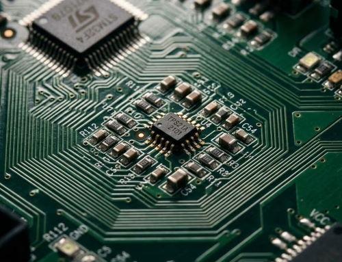
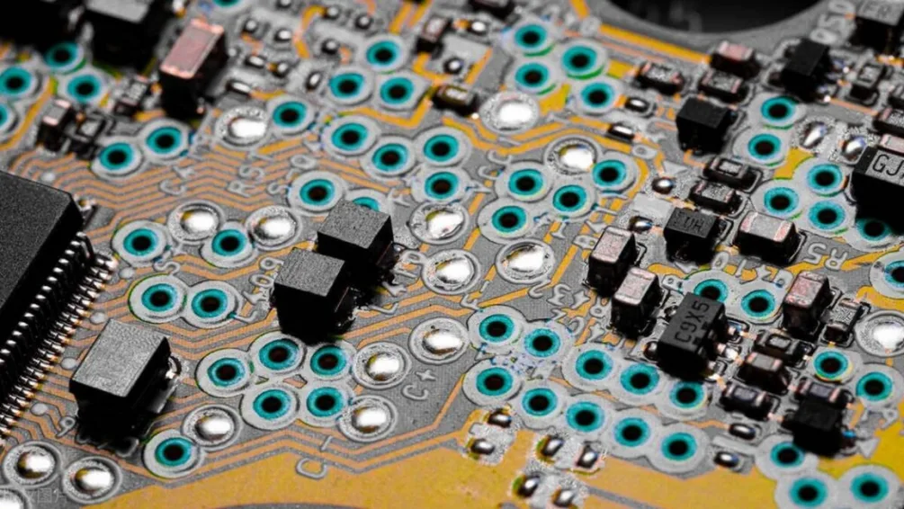
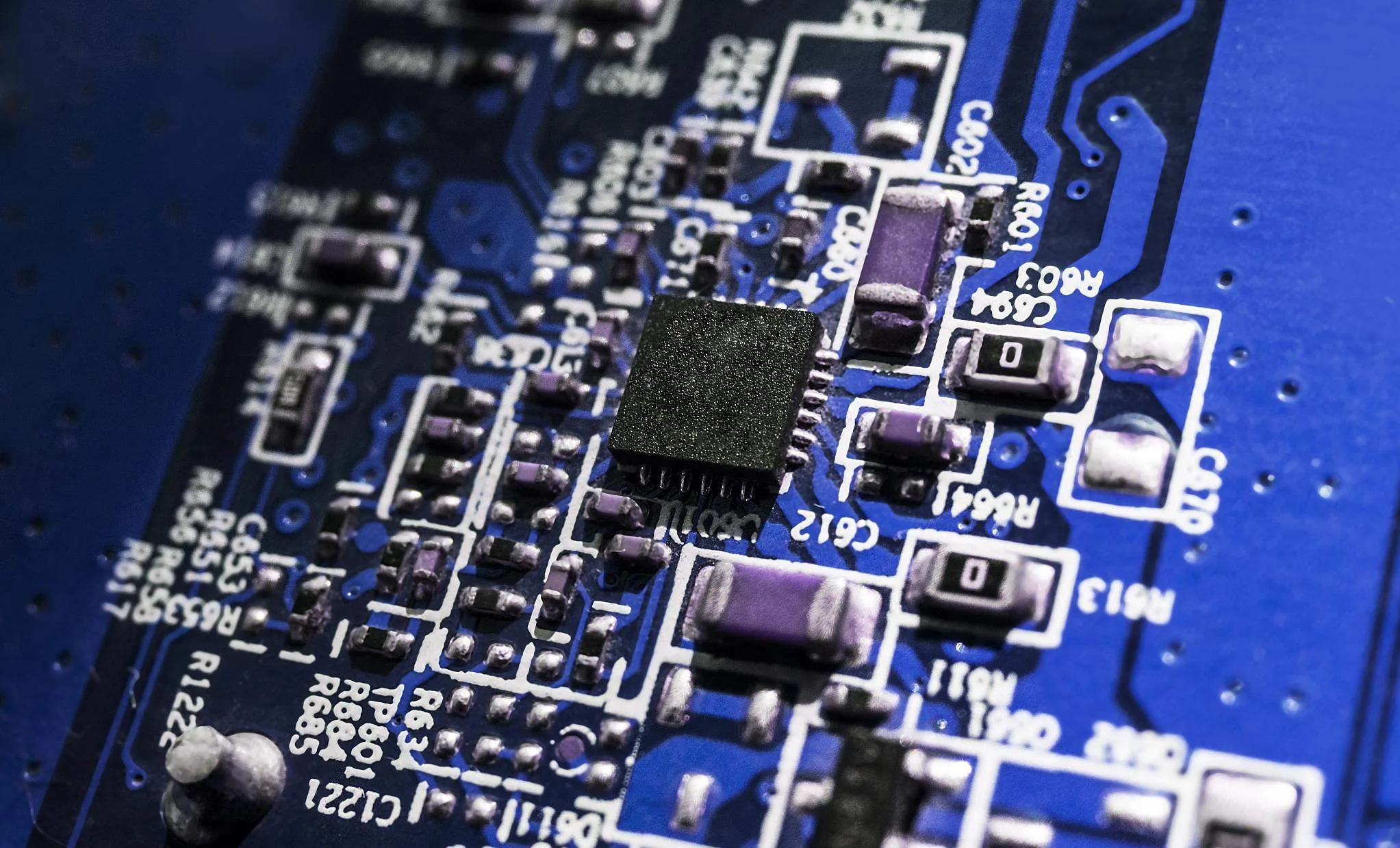
3. SMD Package: The Rise of Surface Mount Technology (SMT)
SMD package is a surface mount device technology whose core feature involves directly soldering electronic components onto the surface of a printed circuit board (PCB) through leadless or short-lead designs, eliminating the need for through-hole mounting.
3.1 What are the Technical Advantages of SMD?
Compact Size and Lightweight
SMD features small dimensions, making them ideal for high-density PCB designs. This facilitates product miniaturization and weight reduction, particularly for portable devices such as smartphones and wearables.
High Automation Efficiency
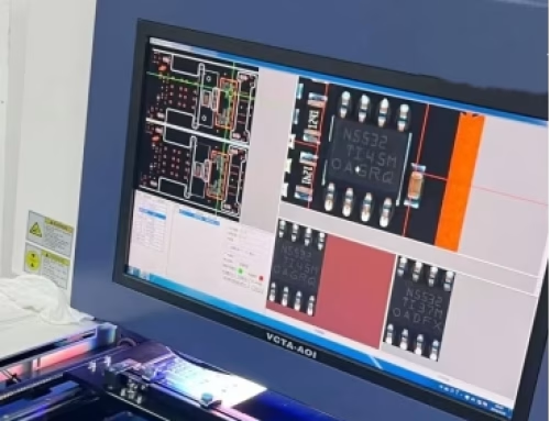
SMD package supports automated production via pick-and-place machines, delivering high manufacturing efficiency for mass production. It ensures stable soldering quality while minimizing human error.
Excellent High-Frequency Performance
SMD components have short pins with low inductance and resistance, which supports micro-packaging (e.g. QFP, BGA). This makes them perfect for use in high-frequency applications, as they can transmit signals and dissipate heat more efficiently.
Superior Shock Resistance
SMD components are directly soldered onto the PCB surface, creating a robust connection. Their shock resistance outperforms DIP, making them suitable for applications in vibrating environments.
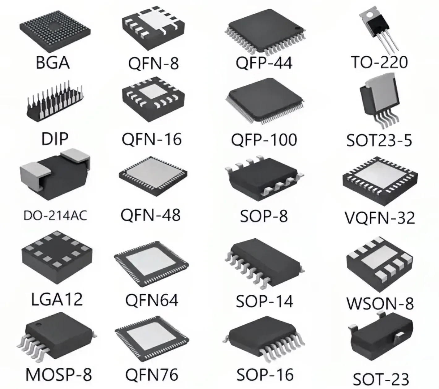
3.2 What are the Primary Types of SMD Package?
(1) Basic Discrete Device Package
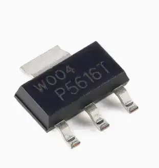
SOT Series
- SOT-23: 3-pin low-power transistor/diode package (power dissipation <300mW), suitable for consumer electronics.
- SOT-89: Medium-power devices (300mW-2W) with heat sink pad, used in power management.
- SOT-223: High-power package (2-50W), a variant of TO-252, suitable for industrial power supplies.
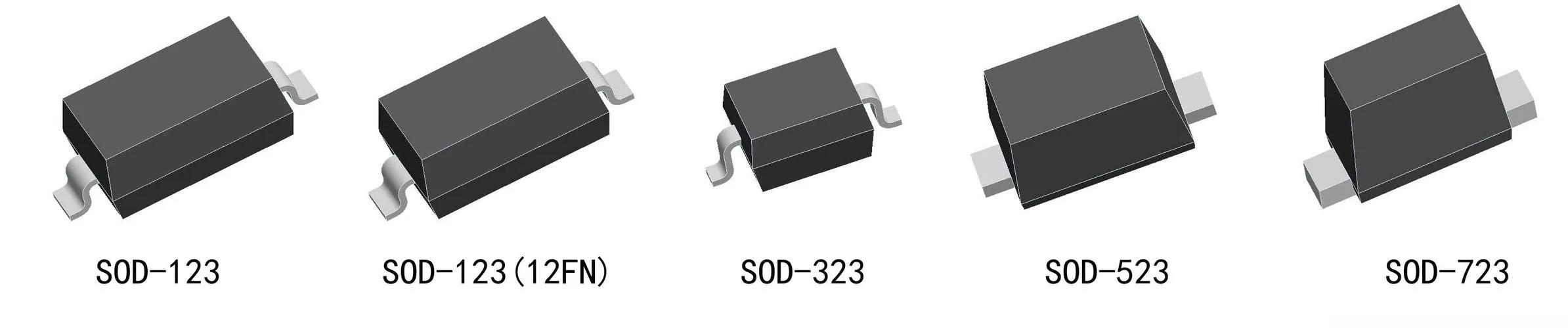
SOD Series
Compact diode packages (e.g., SOD-123) with fast reverse recovery time, used for high-frequency rectification.
(2) Integrated Circuit Package
SOIC/SOP
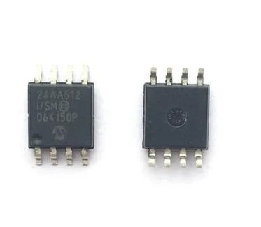
Alternatives to dual in-line packages, with pin pitches of 1.27mm/0.8mm, serving as universal IC packages (e.g., op-amps, logic chips).
Derivative Types: SSOP (Shrink Small Outline Package), TSOP (Thin-Sided Outline Package).
QFP/TQFP
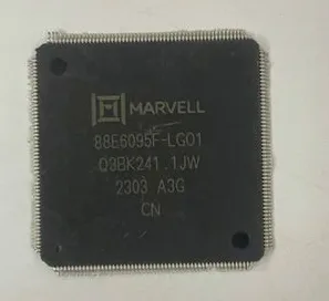
Quad Flat Package with pins on four sides, pin counts 44-160, pitch 0.4mm-1.27mm, used for microcontrollers/FPGAs.
TQFP thickness only 1.2mm, suitable for portable devices.
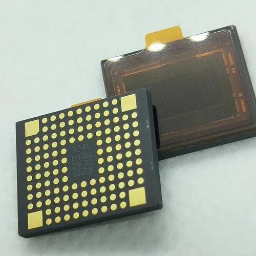
BGA
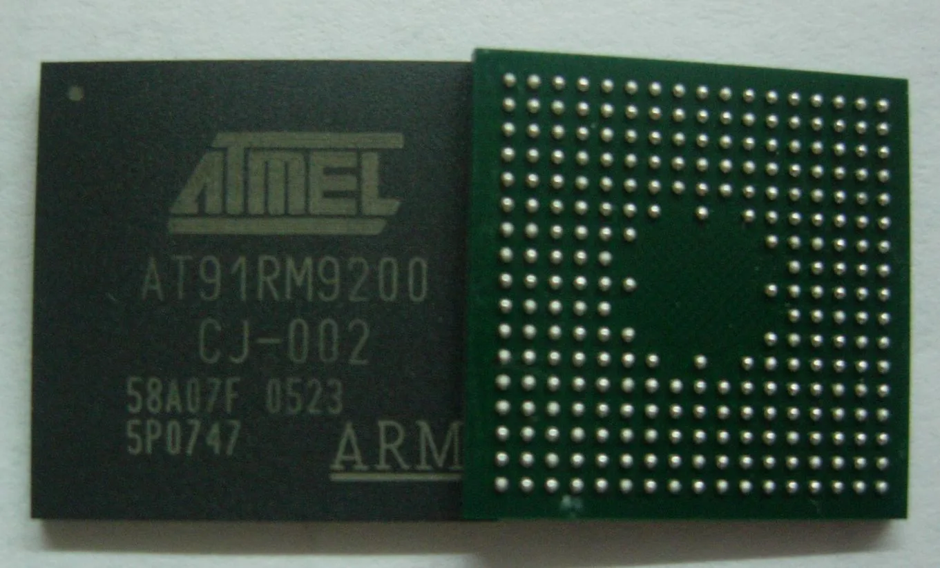
Bottom-ball arrays offer high pin density (e.g., a 360-pin BGA is only 31mm²). They are used for CPUs/GPUs, but require X-ray inspection.
Features:
- Although the number of I/O pins is increased, the pin pitch is much greater than that of QFP, resulting in higher assembly yields.
- The thickness is reduced by more than half, and the weight is reduced by more than three-quarters compared to QFP.
- Parasitic parameters are reduced, signal transmission delay is minimized, and frequency of use is greatly increased.
- Coplanar soldering is supported for assembly, resulting in high reliability.
- Like QFP and PGA packages, BGAs still occupy a significant amount of substrate space.
(3) No-Pin/High-Density Package
QFN (Quad Flat No-Pin)
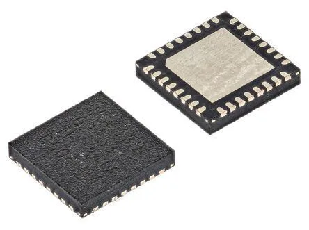
A pinless quad flat package featuring peripheral terminal pads and a chip pad exposed for mechanical and thermal integrity.
Features:
- Pinless pad design occupies minimal PCB area.
- Extremely thin profile (<1mm) for space-constrained electronic applications.
- Ultra-low impedance suitable for high-speed or microwave applications.
- Superior thermal performance due to large bottom heat dissipation pad.
- Lightweight construction ideal for portable devices.
CSP
Chip-scale package (approaching die size), designed for sensors/RF modules, supporting 01005 mounting process.
(4) Special Function Package
PLCC
J-lead quad-lead package with high vibration resistance, used in automotive electronics.
TO-252
High-power SMD package (e.g., MOSFETs), compatible with through-hole heat sink designs.
3.3 Selection Recommendations
High-frequency Circuits: Prioritize QFN/BGA.
High-density Designs: Select 0.4mm pitch QFP or 01005 chip components.
Thermal Requirements: SOT-89/TO-252 or DFN with metal pads.
4. Technical Comparison and Selection Recommendations of Component Package
SMD packages offer compact size and high efficiency, making them suitable for high-frequency portable devices. DIP packages feature low cost and ease of maintenance, making them ideal for small-batch production. Select the optimal solution based on specific requirements.
4.1 Disadvantages of DIP Package
Large Size and Heavy Weight
DIP packages are relatively bulky, making them unsuitable for high-density PCB designs and limiting product miniaturization and weight reduction.
Low Automation Efficiency
DIP package requires insertion machines or manual insertion, resulting in lower production efficiency and unsuitability for mass production.
Poor Vibration Resistance
The long pins of DIP package are susceptible to vibration, potentially causing poor contact or component detachment.
4.2 Disadvantages of SMD Package
High Soldering Process Requirements
SMD package requires high-temperature processes like reflow soldering, placing significant demands on soldering equipment and techniques. Improper soldering may damage components.
Difficult Maintenance
SMD components are small, making disassembly and repair after soldering challenging. Specialized equipment and expertise are typically required.
Higher Costs
SMD package involves higher equipment and process costs, requiring significant initial investment. It is best suited for large-scale production to spread these costs.
4.3 Factors to Consider When Selecting Component Package Type
Component Functionality and Scale: How many pins does the chip have internally? What is its complexity level?
PCB Layout and Density: How large is the board? How many components need to be placed?
Thermal Requirements: High-power devices require better heat dissipation paths (e.g., TO series, thermal pads on QFN/BGA).
Cost: Significant variations exist in material and manufacturing costs across different packages.
Manufacturability/Serviceability: Is it easy to produce and solder? Is it easy to repair if issues arise? DIP is generally easier to repair than SMD (especially BGA).
Electrical Performance: Requirements for impedance and parasitic inductance/capacitance in high-frequency, high-speed signals (e.g., BGA outperforms long-lead packages at high frequencies).
End Product Requirement: Mobile devices like smartphones demand compact size and light weight, necessitating miniaturized SMD; industrial equipment may prioritize reliability and repairability.
5. Future Trends of DIP and SMD Package
DIP is a traditional through-hole packaging technology. SMD technology is gradually replacing it in certain situations. At the moment, DIP packages are mostly used for small-to-medium scale integrated circuits (typically with no more than 100 pins). Due to its larger size and reliance on through-hole soldering processes, it is becoming increasingly marginalized in fields demanding miniaturization, such as consumer electronics. In the future, DIP may persist only in industrial control, educational experimentation, and other scenarios demanding high reliability without requiring high-density integration.
SMD leveraging high integration and automation advantages, has become the mainstream packaging direction. SMD packages like QFP/PFP enable precise connections for large-scale integrated circuits through surface mount technology, meeting high-frequency and narrow-pitch requirements. Future trends include:
High-density Package: FC-BGA (Flip Chip Ball Grid Array) package enhances interconnect density via substrate technology, becoming the preferred choice for high-performance processor packaging;
Heterogeneous Integration: SiP (System-in-Package) substrate technology drives multi-chip modularization, meeting miniaturization demands for wearables, 5G, and other applications;
Material Innovation: Organic packaging substrates (accounting for over 80% of market value) evolve toward thinner profiles and lower loss characteristics, supporting high-frequency applications.
6. Component Package FAQs
Component package refers to a protective enclosure designed to house electronic components for assembly and operation within devices. Various types of component package exist, such as DIP (Dual In-line Package), QFN (Quad Flat No-lead Package), and Ball Grid Array (BGA).
Dual In-line Package, also known as DIP packaging or DIP package, abbreviated as DIP or DIL, is a type of integrated circuit packaging. The integrated circuit has a rectangular shape with two parallel rows of metal pins on either side, referred to as pin headers. DIP-packaged components can be soldered into plated-through holes on a printed circuit board or inserted into DIP sockets.
BGA package is a surface mount technology characterized by a regular array of ball-shaped pins formed on the bottom of the package. This packaging method offers advantages such as large pin pitch, excellent thermal performance, and superior signal transmission capabilities. Consequently, it is widely used in high-speed, high-performance integrated circuits.
A QFN package is a square, flat, pinless surface mount package. Its primary characteristics include compact size, light weight, and excellent electrical and thermal performance. It achieves efficient heat dissipation through a large exposed pad at the package’s center, while multiple contacts around the perimeter facilitate electrical connections.
Heat-sensitive applications: QFN (Quad Flat No-Lead) enhances thermal dissipation via its bottom pads, making it suitable for power devices; metal/ceramic packages (e.g., CBGA) withstand high temperatures and are used in industrial-grade equipment.
On one hand, surface mount components are only one-tenth the size of through-hole components and weigh 60% to 80% less. This means that electronic products can shrink by 40% to 60%. For example, 0805 surface-mount resistors are much smaller than through-hole resistors, with a single bag holding thousands of components. On the other hand, machines can put thousands of pieces in place every hour. This makes production five times more efficient.
7. Summary
The package is the “clothing” and “shoes” of an electronic component, determining how it “stands” (is mounted) on the circuit board. In modern electronics, Surface Mount Technology (SMT) and its various derivative component packages (such as QFP, BGA, QFN, SOT) represent the dominant trend, offering compact size, high density, and superior production efficiency. DIP is primarily used in applications requiring high mechanical strength or efficient heat dissipation (e.g., high-power devices), as well as for maintenance and prototyping.
Table of Contents
- 1. component Package နည်းပညာ ျခံဳငံုသံုးသပ္မႈ
- 2. ရိုးရာအထုပ်e: DIP (Dual In-line Package)
- 3. SMD Package- Surface Mount Technology (SMT) ထွန်းကားလာခြင်း
- 4. နည်းပညာဆိုင်ရာ နှိုင်းယှဉ်မှု နှင့် ရွေးချယ်ရေး အကြံပြုချက်များ Component Package ၏
- 5. အနာဂတ်ရေစီးကြောင်းများ DIP နှင့် SMD Package များ
- 6. အစိတ်အပိုင်းအစုံအလင် FAQs
- 7. အကျဉ်းချုပ်

Get Your PCB Quote!