
From PCB Prototypes to Full Production: The Role of a PCB Board Maker
Get Your PCB Quote!
Table of Contents

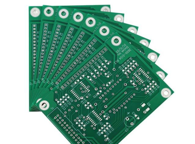
PCBs or printed circuit boards constitute the core of electronic devices of today. Electronic parts suppliers transmit electrical signals to all the electronic components making them come to life.
The steps of PCB design process begin with the design and verification process and proceed to the manufacturing of circuit boards. A lot of steps require guidance from computers and machine-driven equipment to ensure accuracy and to prevent short circuits or circuits that are not complete.
1. Crafting the PCB
The first step of manufacturing of PCBs is design. It serves as a blueprint for PCB manufacturing and design the designer draws out an outline for the PCB that meets all stipulated requirements. The most widely used design exporting software utilized to export designs by PCB designers is known as Extended Gerber — also called IX274X.
Extended Gerber is great PCB design software as it also functions as an output file. It provides all the data that designers and PCB manufacturers need, like the amount of copper layers used and the number of solder masks required, and other components of the notation. Once a design outline is digitized for the PCB by software, all components and elements that make up the plan are inspected to ensure that there aren’t any errors.
2. Design Review and Engineering Questions
Another crucial step in the fabrication process is looking over the design for any potential mistakes or defects, as well as manufacturing problems. Engineers conduct an analysis of the design and looks over each part that makes up the PCB design to ensure that there aren’t any missing components or wrong structures. The design is then moved to the printing stage following approval from the engineer and client. The client may wish to review the working files and confirm the array’s construction tools, holes for tooling and multi-up array orientation scoring as well as snap tabs.
3. Printing Process
PCB makers utilize a customized printing manufacturing process. In contrast to other plans, the procedure requires a special plotter printer to create the PCB film. After printing, the film is in essence a photograph negative that is printed on PCB.
• The plotter prints PCB’s interior layers with two distinct colors of ink:
• Ink black, which indicates PCB’s circuits as well as copper lines
• Clear ink that indicates the PCB’s non-conductive regions similar to the base fiberglass
On the outermost layers in the PCB layout, the pattern is reversed. Clear ink is referring to the lines of copper pathways, however black ink refers to areas in which copper is to be removed.
4. Preparing the copper material for the interior layers
In the fourth step, the electronic parts distributors begin the process of building the PCB. The resist allows engineers to find a perfect match between the photographs of the blueprint and the images printed on the photo resist.
The UV light travels through the translucent areas of film and causing it to harden the photo resist. This is a sign of areas of copper that are to remain as pathways. The black ink blocks light from entering the areas where it isn’t intended to be hardened to allow them to then be taken away.
The layers inside get treated by etch resistance to guard the copper against the etching process. The treatment is completed prior to the core being put through the process of etching. After the etching process is completed, the only copper left is the copper that was intended to be used by the creator.
5. Using Inner Layer to Remove Copper
The inner or core layers that make up the PCB have to be stripped of any excess copper prior to it is possible to continue the PCB manufacturing process is able to proceed. Etching is the process of covering the required copper on the board, and exposes the remainder part of the circuit board chemicals. The chemical etching process eliminates all copper that was not protected from the PCB leaving only the necessary amount.
This process can vary in terms of time or amount of etching solution for copper used. The larger PCBs and those that have heavier structures might require more copper, which results in greater amounts of copper that need to undergo an etching process to remove. Thus, these boards might require more duration or cleaner.
6. Layer Alignment
After technicians have cleaned each layer of PCB they’re now ready for alignment as well as optical examination. The holes made earlier were utilized to align the inner as well as the outside layers. In order to align layers technicians place them on a punching machine referred to by the name of an optical punch. The optical punch moves an axis through the holes in order to align the PCB’s layers.
7. Automated Optical Inspection
Following the optical punch another machine conducts the optical examination to verify that there aren’t any flaws. This optical inspection process is crucial because, after the layers have been put together, any mistakes present can’t be fixed. To ensure that there are no flaws to ensure that there are no defects, the AOI machine will compare the PCB to an Extended Gerber design, which is the model used by the manufacturer.
The AOI process is essential to the functioning of printed circuit board components. If it is not done, the boards be short circuited, don’t comply with the design specifications, or contain extra copper that wasn’t eliminated during etching can go through the remainder of the procedure.
8. Laminating the PCB Layers
In step 8 in step eight, the initial piece of the substrate also covered with an aluminum foil that contains the etchings of the copper trace. When the outer and inner layers are in place and pressed together, it’s the time to press the two layers together. The dielectric layer is inserted between the inner core and outer layers.
The layers are joined with clamps made of steel and a specially-designed press table. Each layer is able to be inserted into the table with a specially designed pin. The person who is performing the laminating procedure begins with the placement of a layer pre-coated epoxy resin referred to as prepare (pre-impregnated) placed on the basin of alignment on which table.
9. Drilling
Prior to drilling, an X-ray machine is employed to identify the drill holes. After that the registration holes or drilling holes are made so that PCBs is secured prior to the holes that are more specific are made. When it’s time to drill the holes using a computer-guided drill, it is employed to create the holes, employing the software of extended Gerber design as a reference.
When the drilling is completed after which any copper left at the edges of the drill is removed.
10. PCB Plating
Once the panel is completed drilling, it is ready to be coated. The plating process utilizes an agent to bond all the layer of PCB.
The bathing process is to coat the panel with the thickness of a micron thick layer of copper. It is then deposited over the top layer and down into the holes which have just been made.
Prior to filling the holes using copper let the fiberglass substrate which forms the panel’s interior. The component copper bathing protects the walls that were drilled earlier.
Summary
Quality engineering and production of PCBs are essential components of the electronic circuit board’s operation. Understanding the complexity involved in the manufacturing process as well as how each stage must be completed provides a greater understanding of the expense and time that goes into every printed circuit board.
Table of Contents

Get Your PCB Quote!


