HASL vs. ENIG: A Best Guide to PCB Surface Finish
HASL and ENIG are two different surface finish technologies in the electronics industry and are widely used in the field of PCB manufacturing.
Get Your PCB Quote!

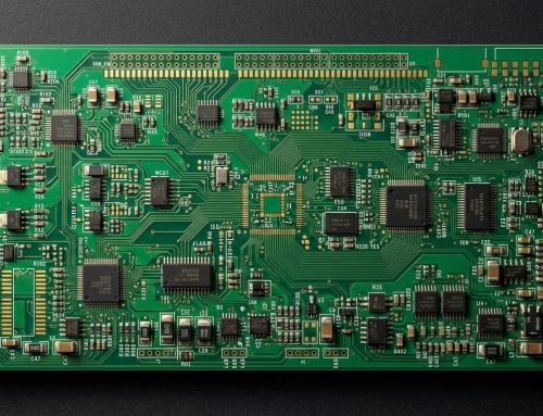
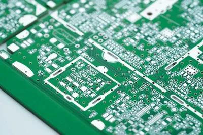
HASL and ENIG are two common surface treatments that are used to protect the leads and pads of PCB boards. These treatments can make the boards more conductive and reliable. We all know that the process for making printed circuit boards (PCBs) is very important. It directly affects the quality and placement of the finished PCB board. The following is a detailed description of the two methods. It includes the process, advantages, and disadvantages, as well as how they are applied.
1. What is HASL or Hot Air Solder Leveling?
HASL (Hot Air Solder Leveling) is a popular PCB surface finish. It creates a coating that protects the copper layer and allows it to be soldered. The main idea is to expose the copper surface of the circuit board that is immersed in a molten tin alloy solder tank. Then, through high-speed hot air scraping, remove excess solder, forming a uniform tin layer.
1.1 Process Flow
1) Pre-treatment
①Degreasing and Cleaning: Alkaline detergent removes oil, fingerprints, and other organic pollutants. This keeps the copper surface clean.
②Micro-etching Roughening: Acid etching solution slightly corrodes the copper surface, forming a microscopic rough structure, to enhance the adhesion of solder.
③Activation Treatment: Hydrochloric acid removes oxide film and activates copper surface activity.
2) Spray Tin Core Operation
①Dip Tin: PCB immersed in molten solder tank (leaded process: 245-260 ℃, lead-free: 260-275 ℃), stays 3-5 seconds to make the solder cover the surface and hole walls. -5 seconds, so that the solder covers the surface and the hole wall.
②Hot Air Leveling: high-pressure hot air knife (wind speed 60-80m/s, angle down 4 °) to blow away excess solder, control the thickness of the tin layer (usually 1-3μm) and flatness.
3) Post-processing
①Washing and Drying: Remove residual flux and prevent corrosion.
②Quality Inspection: check the thickness, uniformity, bridging, and other defects of the tin layer.
1.2 Main Types
PCB HASL process is mainly divided into the following two types. The core difference lies in the lead content and environmental protection:
1) Lead-Based HASL
Ingredients and Characteristics
Tin-lead alloy (lead content of about 37%), the element of lead can enhance the soldering activity and reduce the eutectic temperature to 183 ℃. Good fluidity during soldering, high mechanical strength, and bright surface.
Disadvantages
Lead is toxic and harmful to human health. It also doesn’t meet environmental standards. Poor process flatness and high-density components (e.g., BGA) are susceptible to false soldering or short circuits due to uneven pads.
2) Lead-Free HASL
Composition and Characteristics
Tin-based alloy (lead content ≤ 0.5%), RoHS compliant. Higher melting point (e.g. SnAgCu eutectic temperature 217℃), better mechanical strength of soldered joints, but lower surface gloss.
Disadvantages
The soldering temperature needs to be higher (247~267℃), and the process is more complex. The cost is slightly higher than that of leaded spray tin.
1.3 Advantages and Disadvantages
1) Core Advantages
Significant Cost-effectiveness
Simple equipment, material cost is much lower than the process of immersion gold and immersion tin, suitable for mass production and cost-sensitive products (e.g., consumer electronics).
High Soldering Reliability
The tin layer is made up of the same materials as the solder paste. This creates a strong intermetallic compound (IMC), which reduces the risk of false soldering and cold soldering.
Oxidation Resistance and Storage Stability
The tin layer protects the copper from the air and moisture, which can cause it to oxidize. The shelf life of tin-coated copper is up to 6-12 months at room temperature. This is longer than the shelf life of copper that has been processed using the OSP method.
Wide Applicability
HASL is compatible with common substrates such as FR-4, CEM-3, etc., and supports through-hole components and large pitch wires (>0.5mm) well.
Excellent Detectability
A bright silver-colored tin layer makes it easy to check for problems. It can be checked automatically with machines (AOI) to quickly find problems like copper leakage and short circuits.
2) Main Limitations
Insufficient Flatness
Vertical tin spraying can cause “tin droop” because of gravity and the uneven thickness of the pads (typical difference ± 25%). This can result in SMT patch offset or monument, making it difficult to meet the BGA, QFN, and other high-density packaging requirements.
High-Temperature Process Risk
Spray tin temperature needs to reach 245-300 ℃ (leaded/lead-free), which may damage heat-sensitive components or lead to plate deformation.
Environmental and Process Defects
Leaded Pollution: Leaded tin spraying generates heavy metal waste, which needs to be specially disposed of and does not comply with the RoHS directive.
Porosity and Tin Beads: The tin spray layer can have tiny holes, and tin beads are easily formed when the tin is remelted during double-sided SMT assembly. This increases the risk of short-circuiting the fine pins.
1.4 Application Scenarios
PCB HASL is a process that is used a lot in the following situations because it is inexpensive and reliable:
1) General Electronic Product Manufacturing
Consumer Electronics
Such as common household appliances, chargers, toys, and other cost-sensitive products. The tin spraying process ensures basic soldering reliability while significantly reducing production costs, making it suitable for high-volume manufacturing.
Through-Hole Terminal Technology (THT) Scenario
The higher thickness of the tin spray layer provides sufficient tin for the pin soldering of traditional through-hole components (e.g., sockets, capacitors, relays) and enhances the mechanical strength and electrical conductivity.
2) Circuit Boards with Specific Design Requirements
Large Pitch Leads and Pad Design
PCBs with large lead spacing (usually >0.2mm) or large pad sizes, the flatness of the spray tin process has less impact, and can meet soldering requirements.
Non-HF/High Speed Signal Transmission Boards
There are microscopic unevennesses on the surface of the spray tin that may affect the high-frequency signal integrity, so it is more suitable for low-frequency circuits such as audio equipment and power supply boards.
3) Cost Control Priority Items
Mass-produced Industrial Control Boards
Spray tin can balance performance and cost. This is useful for industrial equipment like motor controllers and PLC modules. These are important for industrial processes, but they don’t need to be extremely precise.
Low and Medium Density Wiring Design
High-density boards (e.g., BGA dense packages) require higher flatness, and tin spraying can lead to false soldering. Low and medium-density boards (e.g., double-sided boards) are not subject to this limitation..
4) Scenarios where HASL is not applicable
High-precision BGA/CSP Packages: high pad flatness is required, and processes such as immersion gold are needed.
High-frequency/High-speed Circuits: such as 5G communications, RF modules, and tin spray surface roughness may cause signal loss.
Long-term Exposure Environment: The antioxidant property of the tin layer is weaker than that of gold and ENIG. It is also more susceptible to oxidation in humid or corrosive environments.
2. What is ENIG or Electroless Nickel Immersion Gold?
The PCB HASL process uses hot air to level the pad surface. This forms a tin layer that protects the copper surface. The ENIG process is completely different. ENIG (Electroless Nickel Immersion Gold) is a process that covers the copper surface of a circuit board with a layer of nickel and gold. This process is used to make soldering more reliable and to improve resistance to oxidation and conductivity.
2.1 Process Flow
1) Pre-treatment (Surface Cleaning and Activation)
① Degreasing
Use an alkaline solution (e.g., 30% AD-482) to remove oil, fingerprints, and oxides from the copper surface to ensure a clean surface.
② Micro-etching
Use a mixture of sodium persulfate (60g/L) and sulfuric acid (2%) to form a slightly rough copper surface and enhance the bonding force. The micro-etching rate should be strictly controlled at 25-40μ inches.
③Activation and Post-dip
Activation: Dip into a solution containing palladium catalyst (e.g., 10% Act-354-2) to adsorb palladium nuclei on the copper surface as a reaction center for nickel deposition.
Post-dip: Weak acid cleaning (1% H₂SO₄) to remove residual impurities and prevent palladium inactivation.
Critical Controls: Activation solution copper content > 800ppm needs to be replaced; each tank is maintained weekly.
2) Electroless nickel plating (to form nickel-phosphorus alloy layer)
Composition of Plating Solution: containing nickel salt, reducing agent (sodium hypophosphite), complexing agent, and stabilizer.
Process Parameters:
① Temperature: 85-90°C (reduced to 70°C to retard aging after shutdown)
② pH: 5.3-5.7
③ Thickness: 3-5μm (controlled by time, generally 2-4 minutes).
④ Impurity control: heavy metals such as lead and tin will inhibit the reaction and need to be strictly filtered.
3) Gold Immersion (gold layer deposited by replacement reaction)
Reaction Principle: Nickel and gold ions undergo a replacement reaction (Ni + 2Au⁺ → 2Au + Ni²⁺), forming a dense gold layer on the surface of the nickel layer.
Plating Solution Conditions:
①Au salt concentration: 1.5-3.5g/L
②Temperature: 85-90℃
③pH value: 4-5
Gold Layer Characteristics: The thickness is usually 0.025-0.1μm (1-4μ inches), and uniform crystallization is required to safeguard solderability.
4) Post-processing (Cleaning & Drying)
① Waste gold water washing: Recover the residual gold solution.
② High-pressure water washing: 30-50PSI pressure to remove the liquid in the hole.
③ Acid washing and drying:
Sulfuric acid (10%) + hydrogen peroxide (30g/L) to remove organic matter thoroughly;
DI water rinse and hot air drying, the gold layer is bright and oxidation-free.
2.2 Advantages and Disadvantages
1) Core Advantages
Excellent Soldering Performance
Immersion gold’s crystal structure is dense and flat, which makes it great for precision soldering, like BGA. It’s also better than other methods like spraying tin or OSP because the solder joints are stronger, which reduces the risk of false soldering;
A nickel layer is used as the bottom layer to help the gold layer stick better, and to prevent the pad from oxidizing and causing soldering problems. The nickel layer acts as a base layer to enhance the bonding force of the gold layer and prevent soldering defects caused by pad oxidation.
Stable Electrical Performance
The gold layer has excellent electrical conductivity (low resistance), and the skin effect has no effect on signal transmission, which is suitable for high-frequency circuits.
It resists oxidation, can handle being in humid environments, and is reliable..
Good Surface Quality
Bright and bright colors, uniform and smooth plating, enhance the product’s appearance;
The connector’s nickel-gold alloy layer is more durable and resistant to wear than pure gold plating. This layer helps extend the life of the connector when it is inserted and removed;
Soldermask and copper surface bonding is more solid, reducing the risk of micro-short-circuit.
2) Main Limitations
High Cost
Gold price fluctuation, the cost of gold immersion is about 10 times that of the OSP process, and the process complexity is high.
Difficulty of Process Control
Prone to defects such as “seepage plating” (deposition of nickel and gold to non-pad area), “black plate” (corrosion of nickel layer leading to soldering failure), and the yield rate is dependent on fine control.
In high temperatures (like when soldering for a long time), the gold layer might spread to the copper base. This could cause a short circuit between the pads.
Limited Application Scenarios
Requires very high cleanliness of the substrate, and slight contamination will lead to poor plating.
Too thin a gold layer (<0.25μm) is prone to pinholes, too thick (>0.1μm) is costly and brittle.
2.3 Application Scenarios
1) Highly Reliable Electronic Equipment
Aerospace and Aviation Equipment
Satellites, rocket control systems, etc., need to withstand extreme temperature changes and a strong radiation environment. The immersed gold layer is chemically stable (gold is not easy to oxidize), and the nickel-gold alloy layer can effectively block the diffusion of copper substrate to ensure the long-term stability of signal transmission.
Medical Life Support Equipment
Pacemakers, medical monitors, etc., have zero tolerance for circuit failure. The ENIG process provides a uniform coating (approx. 0.1-5 microns) that avoids the risk of tin whisker short circuits associated with the HASL process and is resistant to corrosion by body fluids.
2) High Frequency/Precision Signal Transmission
5G Base Station and High-end Router
High-frequency signals require very high impedance consistency. The low surface roughness of immersion gold (Ra<0.1μm) significantly improves signal integrity and reduces high-frequency loss compared to the tin spray process (Ra>1μm).
Gold Finger Connectors
Plug-in interfaces for memory sticks, graphics cards, etc., need to withstand 10,000 times of plugging and unplugging. The high hardness of the immersion gold layer (HV300-400) is better than gold plating, and the contact resistance is stable, ensuring the reliability of repeated connections.
3) Miniaturized high-density electronic products
BGA/CSP Package Chip Soldering
The spacing between mobile phone processors, graphics card chips, and other components is very small. (Sinking gold surface flatness error is only ±0.1μm, especially suitable for the bottom of the non-visible solder joints of the return to repair difficult scenarios.)
Flexible Printed Circuit Board (FPC)
Folding screen cell phone hinge area lines need to withstand bending. Immersion gold has better ductility than hard gold plating, and the nickel layer cushions the stress and prevents the plating from cracking when bending.
4) Severe Environment Industrial Equipment
Automotive Engine Control Unit (ECU)
need to work in -40 ℃ ~ 150 ℃ temperature cycle. Immersion gold layer at high temperatures to inhibit the diffusion of copper atoms (spray tin will accelerate the growth of IMC), to avoid solder joint embrittlement cracking.
Marine Exploration Equipment
A high salt spray environment requires strong corrosion resistance. The dense crystal structure of the immersion gold layer separates water and oxygen. The nickel layer acts as a sacrificial anode to further protect the copper substrate. This improves the life expectancy by more than 3 times compared with the OSP process.
3. Difference between HASL and ENIG
| Features | HASL | ENIG |
| Surface Flatness | Uneven tin layer,
easy to form a “crescent-shaped” pads, affecting the placement of fine-pitch components (eg, BGA) |
Mirror level Surface
flatness, suitable for ≤ 0.5mm fine pitch pins and micro components |
| Soldering Reliability | Thick tin layer, high mechanical strength; but easy to produce tin beads lead to short circuit | Soldering strength is low, nickel-gold interface may
occur “black disk effect” (nickel layer cracking) |
| Oxidation Resistance | Tin layer is easy to oxidize, storage period ≤ 6 months | Gold layer has strong oxidation resistance, storage period ≥ 12 months |
| Signal Integrity | Signal loss at high frequency is high (uneven surface) | Nickel layer shielding +
low resistance of gold layer, excellent high-frequency performance |
| Environmental Protection | Lead-free process is RoHS compliant, but production energy consumption is high | Chemical deposition has no
high temperature link, waste liquid needs to be professionally handled |
| Cost | About 1/3-1/2 of ENIG | High cost (gold + complex
process) |
To understand why some engineers prefer HASL while others insist on ENIG, we must look at the Intermetallic Compound (IMC). The IMC is the chemical bond formed between the solder and the PCB pad.
* HASL Reliability: Because HASL uses a molten tin alloy, it creates a robust Cu6Sn5 IMC layer directly on the copper, providing excellent mechanical strength.
* ENIG Precision vs. Risk: ENIG offers a flat surface ideal for BGA components, but the IMC forms on a nickel base Ni3Sn4. If the electroless nickel process is not strictly controlled, it can lead to the “Black Pad” phenomenon—a brittle phosphorus-rich layer that causes solder joint failure.
Choosing the right finish is not just about cost; it is about managing the microscopic chemistry of your solder joints.
4. HASL & ENIG FAQs
The finish of a PCB depends on its intended use, environmental factors, and budgetary constraints. You can use any finish as long as it meets your requirements, as each finish has its own advantages for different applications.
Yes: ENIG’s ultra-flat surface (Ra<0.1μm) reduces signal scattering, and the excellent conductivity of the gold layer (resistivity of only 2.44μΩ-cm) makes it suitable for high-frequency circuits above 40 GHz.
If the tin layer is not even, it can cause the impedance to change by more than 5%, which is not good. You should not use it for signals above 10 GHz. However, the impact on low-frequency consumer electronics (for example, home appliance control panels) is less.
The HASL process is simple and cost-effective. The process involves immersing the board in a bath of molten solder and then blowing the excess solder off the surface of the board with hot air. This results in a smooth, flat surface that is ideal for through-hole soldering.
The thickness of the PCB surface treatment depends on the specific requirements and type of treatment. For example, the thickness of the nickel layer in an ENIG treatment is between 120 and 240 micrometers, while the thickness of the gold layer is typically between 3 and 8 micrometers. The thickness of the HASL treatment varies depending on the board design and the temperature of the solder bath.
Cost-sensitive products (e.g., consumer electronics power modules);
Dual-sided/through-hole plug-in boards that do not require high-density placement;
Preferred scenarios for wave soldering processes.
Note: Lead-free HASL tin has a higher melting point (217-227°C) and may affect heat-sensitive devices.
High-frequency/high-speed circuits (5GHz+ signals, low conductive loss of the gold layer);
Miniaturized designs (e.g., cell phone motherboards, BGA packages);
Industrial equipment requiring multiple reflow or long storage cycles.
Risk warning: deviation of phosphorus content of nickel layer may cause “black disk” (solder joint brittle crack), and needs to be strictly controlled.
It is feasible, but you need to be careful. For example:
ENIG is used for the main board chip area to ensure precision, while HASL is used for peripheral circuits to reduce cost;
Limitations: Step-by-step processing is required to avoid cross-contamination, and impedance continuity may be affected.
5. Summary
HASL and ENIG are two different technologies used to treat surfaces in the electronics industry. They have many uses, such as in electronic assembly and PCB manufacturing. HASL is a good choice for many standard applications because it is affordable and easy to find. ENIG provides a reliable, flat, and durable finish that is especially suited to long-term, high-density, and complex assemblies. For most applications, ENIG may be the better choice, despite its higher cost.

Get Your PCB Quote!