
Step-by-Step Process of Printed Circuit Board Assembly
PCB assembly involves stenciling, component placement, reflow soldering, inspection, through-hole insertion, and final functional testing.
Get Your PCB Quote!

Electronics is a part of everyday life. Electronic components are set up in everything from our smartphones to automobile. The printed circuit board (also known as PCB) is at the core of all electronics. Most people can recognize PC board assembly. You’ll find these small chips, covered with lines and copper components, at the core of all gutted electronic devices. These boards, made with copper lines, fiberglass and other metal components, are held together by epoxy and insulated using a solder mask. Solder mask is the main reason of green color characteristic.
Here is the PC Board Assembly Manufacturing Process
Step 1: Stenciling with Solder Paste

The process begins with the application of solder paste onto the PCB using a precision stencil made of stainless steel. This step is comparable to screen printing, where the paste is deposited only onto specific pads where components will be mountedThe stencil allows the assembler to only apply solder to specific parts of the PCB. These are the parts where the components will be placed on the final PCB.
Solder paste is a grayish substance made up of small metal balls, or solder. The small solder spheres combine 96.5% tin with 3% silver and 0.5% copper to create a dependable SAC305 alloy suitable for high-performance electronics. Solder paste is made by mixing solder and flux. Flux functions as a chemical agent to eliminate oxidation while improving solder wetting on metal surfaces. Solder paste is a gray paste that must be applied in the correct amounts and at the right locations.
The solder paste process achieves precision by mechanically fixing the PCB and the stencil together. The solder paste is then applied in precisely measured amounts by an applicator. The apparatus distributes paste uniformly throughout the stencil. The solder paste is still in the correct locations after removing the stencil.
Step 2: Select and Place
The PCB board assembly process continues with the pick-and-place machine. A robotic device places SMDs (surface mount devices) on the prepared PCB. The majority of PCB components are not connectors. The SMDs will then be soldered to the surface of PCBs in the following step.

Formerly human operators were responsible for manually picking up and placing each component during assembly. This step, thankfully today, is automated by PCB manufacturers. Machines demonstrated greater accuracy and consistency than humans which prompted the shift. Humans can work fast, but fatigue and eye strain tend to develop after a few minutes of working with small components. Machines can work continuously without fatigue.
Step 3: Reflow Soldering Method
The surface mounted components and solder paste must remain in their place. Solder paste must solidify to adhere components to the board. This is achieved by a PCB assembly process known as “reflow”.

The PCBA Circuit Board will be transferred onto a conveyor after the pick-and-place process is complete. The reflow-oven into which the conveyor belt passes appear identical to a pizza oven in size and shape. This oven is made up of series heaters that gradually heat the board at temperatures of around 250 degrees Celsius or 480 Fahrenheit. The solder pastes melts because of the extreme heat inside the oven.
The PCB will continue to move in the oven once the solder has melted. The PCB passes through a series cooler heaters that allow the solder to solidify and cool in a controlled way. It creates a solder joint that is permanent to connect the SMDs with the PCB.
PCBAs, particularly those with two- sided PCB Assembly, require special attention during flow.
Step 4: Inspection & Quality Control
Movement during the flow will frequently affect in a poor connection or no connection. This movement can also cause shorts, since misplaced components may connect circuit portions that shouldn’t be connected.
- Manual Inspection: Despite an upcoming trend towards automated and smart manufacturing processes, manual checks still play a role in PCB assembly. In smaller batches, a designer can perform a visual inspection in person to check the quality of the PCBs after the reflow. This method becomes less accurate and more impractical as the number boards inspected increases. Overlooking such small components can cause optical fatigue and lead to less accurate inspections.
- Automatic Optical Inspect: This is the best inspection method when inspecting large batches of PCBAs. A machine that uses high-powered cameras, known as an AOI, is used to inspect PCBs. The cameras are positioned at different angles in order to see solder connections. The AOI can distinguish between different solder quality connections by the way they reflect light. This is able to do this at high speeds, which allows it to process large quantities of PCBs quickly.
Step 5: Inserting Through-Hole Components

PCBAs can include components other than SMDs. They include components with plated through holes, also known as PTH components.
The plated-through-hole represents a full hole on the PCB that has received a plating coating. These holes are used by PCBA Circuit Board components to transmit signals from one side to the other of the board. Soldering paste is useless in this situation, since it will simply run through the hole.
In the later assembly of PCBs, PTH components will require a different type of soldering technique.
- Manual Soldering- The manual insertion of through-hole components into a PCB is an uncomplicated operation. One person will typically insert one component at a time into a PTH. After they finish, the board will be transferred to the next location, where another worker is inserting the component.
- Wave soldering- It functions as an automated alternative to manual soldering yet employs a distinct operational method. The board is then placed on another conveyor belt after the PTH component has been installed. The conveyor belt is now run through a special oven, where a wave molten solder is sprayed over the bottom of each board.
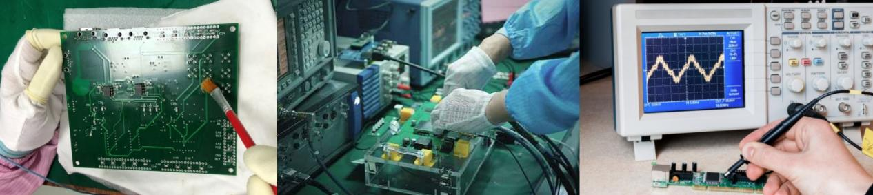
Step 6: Final Product Testing
The PCBA Process reaches completion with a final inspection immediately after the soldering stage concludes. After this step the PCB will function correctly. The “functional test” is the name of this inspection. The test replicates typical operational conditions for a PCB. This test runs simulated and real signals through the assembly of Printed Circuit Boards while testers check its electrical characteristics.

The PCB will fail the test if any of the characteristics (voltage, current, or signal output) show unacceptable fluctuations or reach peaks outside a predetermined area. The PCB that fails the test can be recycled or scrapped depending on company standards.

Get Your PCB Quote!


