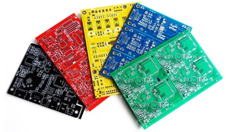
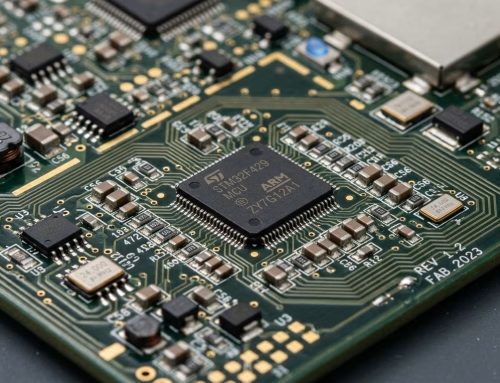
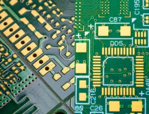
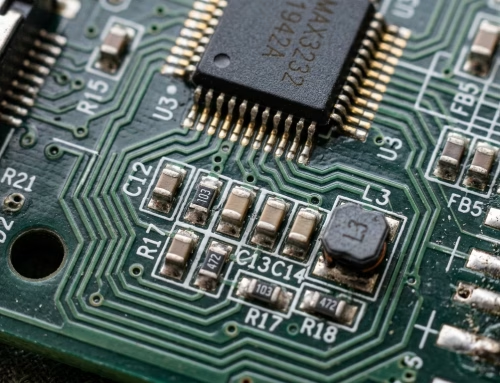
Summary of SMT Quality Issues During PCBA Manufacturing
Get Your PCB Quote!
Table of Contents
- Први вообичаени дефекти и решенија во процесот на издавање
- Второ печатење паста за лемење и анализа на квалитет на лепенка
- SMT анализа на квалитет
- Трето, Влијание врз факторите за квалитет на лемење со преточување
- Четврто, SMT дефекти во квалитетот на заварувањето-Дефекти и решенија во квалитетот на повторното обновување
- Петто, Дефекти и решенија за квалитет на лемење со бранови
- Шесто, меурчиња на ПХБ подлогата по SMA заварување
- Седмо, отворено коло или спој за ладно лемење по заварување со IC иглички
First Common Defects and Solutions in the Dispensing Process
1. Wiredrawing/Tailing
(1)Wiredrawing/tailing is a common defect in dispensing. Common causes include too small inner diameter of the nozzle, too high dispensing pressure, too large distance between the nozzle and the PCB, expired or poor quality of the patch glue, too good viscosity of the patch glue, failure to return to room temperature after being taken out of the refrigerator, too much dispensing amount, etc.
(2)Solution: Replace the nozzle with a larger inner diameter; reduce the dispensing pressure; adjust the “stop” height; change the glue and choose a glue with appropriate viscosity; the patch glue should be restored to room temperature (about 4h) after being taken out of the refrigerator before being put into production; adjust the dispensing amount.
2. Nozzle Blockage
(1)The fault phenomenon is that the nozzle output is too little or no glue is dispensed. The cause is generally that the pinhole is not completely cleaned; impurities are mixed in the patch glue, and there is a hole blockage phenomenon; incompatible glues are mixed.
(2)Solution: Replace with a clean Needle; change to good quality patch glue; the patch glue brand should not be wrong.
3. Empty Printing
(1)the phenomenon is that there is only glue dispensing action, but no glue output. The cause is that the patch glue is mixed with bubbles; the glue nozzle is blocked.
(2)Solution: the glue in the injection barrel should be debubbled (especially the glue installed by yourself); replace the glue nozzle.
4. Component Displacement
(1) the phenomenon is that the component is displaced after the patch glue is cured, and in severe cases, the component pins are not on the pad. The cause is uneven glue output of the patch glue, such as one more and one less in the two glue points of the chip component; component displacement or low initial adhesion of the patch glue during patching; the PCB is placed for too long after dispensing and the glue is semi-cured.
(2)Solution: check whether the glue nozzle is blocked, eliminate the phenomenon of uneven glue output; adjust the working state of the patch machine; change the glue; the PCB should not be placed for too long after dispensing (shorter than 4h)
5. It Will Fall off After Wave Soldering Pieces
(1)The phenomenon is that the bonding strength of components after curing is not enough, lower than the specified value, and sometimes the chips will fall off when touched by hand. The cause is that the curing process parameters are not in place, especially the temperature is not enough, the component size is too large, the heat absorption is large; the light curing lamp is aging; the amount of glue is not enough; and the components/PCB are contaminated.
(2)Solution: Adjust the curing curve, especially increasing the curing temperature. Usually, the peak curing temperature of thermal curing glue is about 150℃. Failure to reach the peak temperature can easily cause the chip to fall. For light-curing glue, it should be observed whether the light-curing lamp is aging and whether the lamp tube is black; the amount of glue and whether the components/PCB are contaminated are issues that should be considered.
6. Component Pins Float up/Shift After Curing
(1)The phenomenon of this fault is that the component pins float up or shift after curing. After wave soldering, the tin material will enter under the pad, and in severe cases, short circuits and open circuits will occur. The main causes are uneven patch glue, Too much glue, or component offset during patching.
(2)Solution: adjust dispensing process parameters; control dispensing amount; and adjust patch process parameters.
Second Solder Paste Printing and Patch Quality Analysis
Solder Paste Printing Quality Analysis
Common quality problems caused by poor solder paste printing include the following:
①.Insufficient solder paste (partial or even overall lack) will lead to insufficient solder in the solder joints of components after welding, the open circuit of components, component deviation, and component erection.
②.Solder paste adhesion will lead to a circuit short circuit and component deviation after welding.
③.Overall deviation of solder paste printing will lead to poor soldering of components on the whole board, such as insufficient tin, open circuit, deviation, vertical parts, etc.
④.Solder paste pull tips can easily cause short circuits after welding.
1. Main Factors Leading to Insufficient Solder Paste
(1)When the printer is working, solder paste is not added in time.
(2) Abnormal solder paste quality, mixed with foreign matter such as hard blocks.
(3)The previously unused solder paste has expired and has been used a second time.
(4)The quality of the circuit board is problematic. There is an inconspicuous covering on the pad, such as solder resist (green oil) printed on the pad.
(5)The fixing clamp of the circuit board in the printer is loose.
(6)The thickness of the solder paste is uneven when it is not printed on the stencil.
(7)The solder paste is not printed on the stencil or there are contaminants on the circuit board (such as PCB packaging, stencil wiping paper, floating in the ambient air foreign matter, etc.).
(8)The solder paste scraper is damaged, and the stencil is damaged.
(9)The equipment parameters such as the pressure, angle, speed, and molding speed of the solder paste scraper are not set properly.
(10)After the solder paste is printed, it is accidentally knocked off due to human factors.
2. The Main Factors Causing Solder Paste Adhesion
(1)Design defects of the circuit board, the pad spacing is too small.
(2)Stencil problem, the hole position is not correct.
(3)Stencil Not wiped clean.
(4)The stencil problem causes poor solder paste shedding.
(5)Poor solder paste performance, viscosity, and collapse.
(6)The circuit board is loosely fixed in the printer.
(7)The pressure, angle, speed, and molding speed of the solder paste scraper are not properly set.
(8) After the solder paste is printed, it is squeezed and adhered to due to human factors.
3. The Main Factors Causing the Overall Deviation of Solder Paste Printing
(1)The positioning reference point on the circuit board is not clear.
(2)The positioning reference point on the circuit board is not aligned with the reference point of the stencil.
(3)The circuit board is loosely fixed in the printer. The positioning ejector pin is not in place.
(4)The optical positioning system of the printer fails.
(5)The solder paste is not printed on the stencil opening and does not match the design file of the circuit board.
4. The Main Factors Causing the Printed Solder Paste to Pull the Tip
(1)Solder There are problems with the performance parameters such as paste viscosity.
(2)There are problems with the molding parameter setting when separating the circuit board from the screen printing plate.
(3)There are burrs on the hole wall of the screen printing plate.
SMT Quality Analysis
Common quality problems of SMT patches include: missing parts, side parts, flipped parts, offset parts, damaged parts, etc.
1. The Main Factors Leading to Missing Patches
(1)The component feeder (feeder) does not deliver the material in place.
(2)The air path of the component suction nozzle is blocked, the suction nozzle is damaged, and the suction nozzle height is incorrect.
(3)The vacuum air path of the equipment fails and is blocked.
(4)The circuit board is poorly purchased and deformed.
(5)There is no solder paste or too little solder paste on the pad of the circuit board.
(6)Component quality problems, the thickness of the same variety is inconsistent.
(7)There are errors in the program called by the patch machine, or the selection of component thickness parameters is incorrect during programming.
(8)Human factors are careless and Bumped off.
2. The Main Factors that Cause SMC Resistors to Flip or Fall Sideways During Patching
(1)The component feeder (feeder) feeds abnormally.
(2)The nozzle height of the placement head is incorrect.
(3)The height of the placement head grabbing the material is incorrect.
(4)The loading hole size of the component tape is too large, and the component flips due to vibration.
(5)The direction of the bulk material when it is placed in the tape is reversed.
3. The Main Factors that Cause Component Patch Deviation
(1) When programming the SMT machine, the X-Y coordinates of the components are incorrect.
(2)The SMT nozzle causes unstable suction.
4. The Main Factors That Cause Damage to Components During SMT
(1) The positioning pin is too high, which makes the position of the circuit board too high and the components are squeezed during SMT.
(2)When programming the SMT machine, the Z coordinates of the components are incorrect.
(3)The nozzle spring of the SMT head is stuck.
Third, Influence on Reflow Soldering Quality Factors
1. Factors Affecting Solder Paste
The quality of reflow soldering is affected by many factors, the most important of which are the temperature curve of the reflow soldering furnace and the composition parameters of the solder paste. The high-performance reflow soldering furnaces commonly used now can accurately control and adjust the temperature curve more conveniently. In contrast, in the trend of high density and miniaturization, the printing of solder paste has become the key to the quality of reflow soldering.
The particle shape of the solder paste alloy powder is related to the welding quality of narrow-pitch devices, and the viscosity and composition of the solder paste must also be selected appropriately. In addition, the solder paste is generally stored in a refrigerated state. When it is taken out, it can be opened only after it returns to room temperature. Special attention should be paid to avoid mixing water vapor into the solder paste due to temperature differences. Use a mixer to stir the solder paste when necessary.
2. The Influence of Welding Equipment
Sometimes, excessive vibration of the conveyor belt of the reflow soldering equipment is also one of the factors affecting the welding quality.
3. The Influence of Reflow Soldering Process
After excluding the solder paste After the quality abnormalities of the printing process and the patch process, the reflow process itself will also cause the following quality abnormalities:
①.Cold welding is usually caused by low reflow temperature or insufficient time in the reflow zone.
②.The temperature rise speed of the tin bead preheating zone is too fast (generally required, the slope of temperature rise is less than 3 degrees per second).
③.The tinned circuit board or components are damp, and excessive moisture can easily cause a tin explosion and tinning.
④.Cracks are generally caused by too fast a temperature drop in the cooling zone (generally, the temperature drop slope of lead welding is less than 4 degrees per second).
Fourth, SMT Welding Quality Defects-Reflow Quality Defects and Solutions
1.Tombstone phenomenon In reflow soldering, chip components often stand up. The reason for the occurrence: The fundamental reason for the tombstone phenomenon is that the wetting force on both sides of the component is unbalanced, so the torque at both ends of the component is also unbalanced, which leads to the occurrence of the tombstone phenomenon.
The following situations will lead to The wetting force on both sides of the component being unbalanced during reflow soldering:
(1)The pad design and layout are unreasonable. If the pad design and layout have the following defects, it will cause the wetting force on both sides of the component to be unbalanced.
①One of the pads on both sides of the component is connected to the ground wire or the pad area on one side is too large, and the heat capacity at both ends of the pad is uneven;
②The temperature difference between various parts of the PCB surface is too large, resulting in uneven heat absorption on both sides of the component pad;
③The temperature at both ends of the pads of small chip components around large devices QFP, BGA, and radiators will be uneven.
Solution: Change the pad design and layout.
(2)There are problems with solder paste and solder paste printing. The activity of the solder paste is not high or the solderability of the component is poor. After the solder paste is melted, the surface tension is different, which will cause the pad wetting force to be unbalanced. The amount of solder paste printed on the two pads is uneven, and the side with more will melt due to the increased heat absorption of the solder paste. Time lag, resulting in unbalanced wetting force.
Solution: Choose solder paste with higher activity, and improve solder paste printing parameters, especially the window size of the template.
(3)Uneven force in the Z-axis direction of patch shift will cause the uneven depth of component immersion in solder paste, and the wetting force on both sides will be unbalanced due to the time difference when melting. If the component patch is shifted, it will directly lead to the tombstone.
Solution: Adjust the process parameters of the patch machine.
(4)Incorrect furnace temperature curve If the reflow furnace is too short and the temperature zone is too few, the working curve for heating the PCB will be incorrect, resulting in excessive wetness difference on the board surface, resulting in unbalanced wetting force.
Solution: Adjust the appropriate temperature curve according to each different product.
(5)Oxygen concentration in nitrogen reflow Nitrogen protection reflow will increase the wetting force of solder, but more and more examples show that tombstone occurs when the oxygen content is too low. The phenomenon of increasing oxygen content is generally considered to be most suitable when the oxygen content is controlled at about (100-500)×10 to the negative sixth power.
2. Tin Beads
Tin beads are one of the common defects in reflow soldering. It not only affects the appearance but also causes bridging. Tin beads can be divided into two categories. One category appears on the side of the chip component, often in the form of an independent large sphere; the other category appears around the IC pins in the form of scattered small beads. There are many reasons for the generation of tin beads, which are analyzed as follows:
(1)Incorrect temperature curve The reflow soldering curve can be divided into four sections, namely preheating, heat preservation, reflow, and cooling. The purpose of preheating and heat preservation is to make the PCB surface temperature rise to 150℃ within 60-90 and keep it warm for about 90. This can not only reduce the thermal shock of the PCB and components but also ensure that the solvent of the solder paste can be partially volatilized to avoid splashing due to too much solvent during reflow soldering, causing the solder paste to rush out of the pad and form tin beads.
Solution: Pay attention to the heating rate and take moderate preheating to make it have a good platform to volatilize most of the solvent.
(2)Quality of Solder Paste
①The metal content in solder paste is usually (90±0.5)℅. Too low a metal content will lead to excessive flux components. Therefore, excessive flux will cause flying beads due to the difficulty of volatilization during the preheating stage.
②Increased water vapor and oxygen content in solder paste will also cause flying beads. Since solder paste is usually refrigerated, when it is taken out of the refrigerator if the recovery time is not ensured, water vapor will enter; in addition, the lid of the solder paste bottle should be closed tightly after each use. If it is not closed in time, water vapor will also enter.
After the solder paste printed on the template is completed, the remaining part should be handled separately. If it is put back into the original bottle, it will cause the solder paste in the bottle to deteriorate and produce tin beads.
Solution: Choose high-quality solder paste and pay attention to the solder paste Storage and use requirements.
(3) Printing and Patching
①In the printing process of solder paste, the template and the pad will be offset. If the offset is too large, the solder paste will flow out of the pad, and tin beads will easily appear after heating. In addition, a poor printing working environment will also lead to the formation of tin beads. The ideal printing environment temperature is 25±3℃ and the relative humidity is 50℅~65℅.
Solution: Carefully adjust the clamping of the template to prevent loosening. Improve the printing working environment.
②The pressure of the Z axis during the patching process is also an important cause of tin beads, but it often does not attract people’s attention. The Z-axis head of some patch machines is positioned according to the thickness of the component. If the Z-axis height is improperly adjusted, the solder paste will be squeezed out of the pad at the moment the component is attached to the PCB. This part of the solder paste will form tin beads during welding. The size of the tin beads generated in this case is slightly larger.
Solution: Re-adjust the Z-axis height of the placement machine.
③The thickness and opening size of the template. If the thickness and opening size of the template are too large, the amount of solder paste will increase and the solder paste will flow outside the pad, especially for templates made by chemical etching.
Solution: Choose a template with appropriate thickness and opening size. Generally, the template opening area is 90℅ of the pad size.
3. Wicking Phenomenon
The wicking phenomenon, also known as the core pulling phenomenon, is one of the common welding defects and is more common in vapor phase reflow soldering. The wicking phenomenon causes the solder to detach from the pad and go up along the pin to between the pin and the chip body, usually resulting in severe cold soldering. The reason for this is that the thermal conductivity of the component pin is large, so the temperature rises rapidly, so that the solder wets the pin first, and the wetting force between the solder and the pin is much greater than the wetting force between the solder and the pad. In addition, the upward warping of the pin will aggravate the occurrence of the wicking phenomenon.
Solution:
(1)For vapor phase reflow soldering, the SMA should be fully preheated before being placed in the vapor phase furnace;
(2)The solderability of the PCB pad should be carefully checked. PCBs with poor solderability cannot be used for production;
(3)Pay full attention to the coplanarity of the components. Devices with poor coplanarity cannot be used for production.
In infrared reflow soldering, the organic flux in the PCB substrate and solder is a good infrared absorption medium, while the pins can partially reflect infrared rays. Therefore, the solder melts first, and the wetting force between the solder and the pad is greater than the wetting force between the solder and the pins. Therefore, the solder will not rise along the pins, and the probability of wicking is much smaller.
4. Bridging
Bridging is one of the common defects in SMT production. It will cause short circuits between components. If bridging is encountered, it must be repaired. There are many reasons for bridging, mainly:
(1)Quality Problems of Solder Paste
①The metal content in the solder paste is too high, especially when the printing time is too long, it is easy to appear Increased metal content leads to IC pin bridging;
②Low solder paste viscosity, flowing outside the pad after preheating;
③Poor solder paste tower drop, flowing outside the pad after preheating;
Solution: Adjust the solder paste ratio or use a better quality solder paste.
(2) Printing System
①Poor printer repetition accuracy and misalignment (poor steel plate alignment, poor PCB alignment). This causes the solder paste to be printed outside the pad, especially the fine-pitch QFP pad;
②Incorrect template window size and thickness design and uneven Sn-pb alloy plating in PCB pad design, resulting in too much solder paste.
Solution: Adjust the printer and improve the PCB pad coating;
(3)Excessive placement pressure, and full flow of solder paste after pressure is a common cause in production. In addition, insufficient placement accuracy will cause component displacement, IC pin deformation, etc.
(4)The reflow furnace heats up too fast, and the solvent in the solder paste does not have time to evaporate.
Solution: Adjust the Z-axis height of the placement machine and the reflow Flow soldering furnace heating speed.
Fifth, Wave Soldering Quality Defects and Solutions
1. Pull tip refers to the excess needle solder at the end of the solder joint, which is a unique defect in the wave soldering process.
Causes: improper PCB transmission speed, low preheating temperature, low tin pot temperature, small PCB transmission angle, poor wave crest, flux failure, and poor component lead solderability.
Solutions: adjust the transmission speed to the appropriate level, adjust the preheating temperature and tin pot temperature, adjust the PCB transmission angle, optimize the nozzle, adjust the wave crest shape, replace the new flux, and solve the lead solderability problem.
2. Causes of cold soldering: poor component lead solderability, low preheating temperature, solder problem, low flux activity, too large pad hole, lead board oxidation, board surface pollution, too fast transmission speed, and low tin pot temperature.
Solutions: solve the lead solderability, adjust the preheating temperature, test the tin and impurity content of the solder, adjust the flux density, reduce the pad hole during design, remove PCB oxides, clean the board surface, adjust the transmission speed, and adjust the tin pot temperature.
3. Causes of thin tin: poor solderability of component leads, too large pads (except for those requiring large pads), too large pad holes, too large welding angles, too fast transmission speeds, high tin pot temperatures, uneven flux coating, and insufficient solder tin content.
Solutions: solve the solderability of leads, reduce pads and pad holes during design, reduce welding angles, adjust transmission speeds, adjust tin pot temperature, check pre-flux device, and test solder content.
4. Causes of leaking solder: poor solderability of leads, unstable solder wave crests, ineffective or uneven flux spraying, poor local solderability of PCB, shaking of the transmission chain, incompatibility of pre-flux and flux, and unreasonable process flow.
Solutions: Solve the solderability of leads, check wave crest devices, replace flux, check pre-flux devices, solve PCB solderability (cleaning or return), check and adjust transmission devices, use flux uniformly, and adjust process flow.
5. After Welding Blistering of Solder Mask on Printed Circuit Boards
After soldering, small light green bubbles will appear around individual solder joints of SMA. In severe cases, bubbles the size of a fingernail will appear, which not only affects the appearance quality but also the performance. This defect is also a common problem in the reflow process, but it is more common during wave soldering.
Cause: The fundamental reason for the blistering of the solder mask is that there is gas or water vapor between the solder mask and the PCB substrate. These trace amounts of gas or water vapor will be entrained in different process processes. When encountering high welding temperatures, the gas expands and causes the solder mask and the PCB substrate to delaminate. During welding, the pad temperature is relatively high, so bubbles first appear around the pad.
The list following reasons all can cause PCB to carry water vapor:
(1)During the processing of PCB, it is often necessary to clean and dry before the next process. For example, after etching, it should be dried before applying the solder mask. If the drying temperature is not enough at this time, water vapor will be entrained into the next process. When encountering high temperatures during welding, Bubbles appear.
(2)The storage environment before PCB processing is not good, the humidity is too high, and the drying process is not timely during welding.
In the wave soldering process, water-containing flux is often used. If the PCB preheating temperature is not enough, the water vapor in the flux will enter the interior of the PCB substrate along the hole wall of the through hole. The water vapor will first enter the area around the pad, and bubbles will be generated when encountering the high temperature of welding.
Solution:
(1)Strictly control each production link. The purchased PCB should be inspected before storage. Usually, PCB should not bubble within 10s at a temperature of 260℃.
(2)PCB should be stored in a ventilated and dry environment, and the storage period should not exceed 6 months;
(3)PCB should be placed in an oven at (120±5)℃ for 4 hours before welding.
(4)The preheating temperature in wave soldering should be strictly controlled. It should reach 100-140℃ before entering wave soldering. If water-containing flux is used, the preheating temperature should reach 110-145 ℃, to ensure that the water vapor can evaporate completely.
Sixth, Bubbles on the PCB Substrate after SMA Welding
Fingernail-sized bubbles appear after SMA welding. The main reason is that the PCB substrate is entrained with water vapor, especially the processing of multi-layer boards. Because the multi-layer board is made of multi-layer epoxy resin semi-cured sheets pre-formed and then hot-pressed, if the storage period of the epoxy resin semi-cured sheets is too short, the resin content is insufficient, and the pre-drying to remove the water vapor is not clean, it is easy to entrain water vapor after hot pressing. Bubbles will also be left because the semi-cured sheets themselves contain insufficient glue and the bonding force between layers is insufficient. In addition, after the PCB is purchased, due to the long storage period and humid storage environment, the patch is not pre-baked in time before production, and the damp PCB patch is also prone to bubbling after patching.
Solution: After the PCB is purchased, it should be inspected and accepted before it can be put into storage; before the PCB is patched, it should be pre-baked at (120±5)℃ for 4 hours.
Seventh, Open Circuit or Cold Solder Joint after IC Pin Welding
Causes:
1.Poor coplanarity, especially for FQFP devices, the pins are deformed due to improper storage. If the placement machine does not have the function of checking coplanarity, it is sometimes difficult to detect.
2.The pin solderability is poor. The IC is stored for a long time, the pins turn yellow, and the poor solderability is the main reason for the false soldering.
3.The solder paste is of poor quality, low metal content, and poor solderability. The metal content of the solder paste usually used for FQFP device welding should not be less than 90%.
4.The preheating temperature is too high, which can easily cause IC pin oxidation and worsen solderability.
5.The size of the printing template window is small, resulting in insufficient solder paste.
Solution:
1.Pay attention to the storage of the device, do not take the components or open the package casually.
2.The solderability of components should be checked during production, especially since the storage period of IC should not be too long (within one year from the date of manufacture), and it should not be subject to high temperature and high humidity during storage.
3.Carefully check the template window size, which should not be too large or too small, and pay attention to matching with the PCB pad size.
Table of Contents
- Први вообичаени дефекти и решенија во процесот на издавање
- Второ печатење паста за лемење и анализа на квалитет на лепенка
- SMT анализа на квалитет
- Трето, Влијание врз факторите за квалитет на лемење со преточување
- Четврто, SMT дефекти во квалитетот на заварувањето-Дефекти и решенија во квалитетот на повторното обновување
- Петто, Дефекти и решенија за квалитет на лемење со бранови
- Шесто, меурчиња на ПХБ подлогата по SMA заварување
- Седмо, отворено коло или спој за ладно лемење по заварување со IC иглички
Get Your PCB Quote!


