
The Whole Process of DIP Plug-in Soldering in Printed Circuit Board Assembly
DIP plug-in soldering ensures reliable PCB connections for high-power components, requiring precise temperature control & quality inspection.
Get Your PCB Quote!
Table of Contents

In the field of electronic manufacturing, PCBA (Printed Circuit Board Assembly) is a crucial link, and the post-soldering process of the DIP (Dual In Package) plug-in is a key step in determining product quality. This article will deeply explore the entire process of DIP plug-in post-soldering in PCBA to help everyone understand the subtleties of this process.
1.Why is DIP Plug-in Post weldingvery Important?
DIP plug-in post-welding is the core process to ensure high-reliability circuit connection, especially in high-power, complex structures, and harsh environment’s electronic product applications. Its quality directly determines the product’s life and safety, and the risk must be strictly controlled through standardized processes (such as temperature control and solder joint detection). As the complexity of electronic products increases, the importance of this process in automotive electronics, industrial equipment, and other fields will continue to highlight.
1.1 Directly Affect the Function and Reliability of PCBA Board
1) Core Guarantee of Electrical Connection Quality
DIP plug-in post-welding realizes the physical connection and electrical conduction between component pins and PCB pads through welding. The quality of solder joints directly determines the stability of signal transmission and the integrity of circuit functions. Defects such as cold solder joints and cold solder joints will lead to poor contact or even functional failure.
2) Important Guarantee of Structural Stability
The mechanical fixation of plug-in components depends on the strength of solder joints, especially in vibration or impact environments (such as automotive electronics). Reliable welding can prevent components from loosening or falling off, ensuring a longer service life of electronic products.
1.2 Necessary Processes for Complex Components
1) Adaptability of High-power/Special Components
For high-power devices (such as power resistors and transformers), high-frequency components or special-shaped packaged devices with high heat dissipation requirements, DIP plug-ins provide stronger mechanical support and heat dissipation paths through through-hole design, which is better than surface mount technology (SMT).
2) The Only Solution for Double-sided Mixed Boards
If there are high components on the A side of the double-sided PCB and the B side plug-in cannot use wave soldering, DIP post-soldering (such as selective wave soldering or dip soldering) is the only effective way to ensure reliable double-sided soldering.
1.3 Key Nodes of Quality Control
1) High-risk Links for Defects
Soldering temperature deviation (standard 350-400℃), improper time control (usually 2-3 seconds) or flux problems can easily lead to defects such as tin tips, pinholes, and cold soldering. The process standards must be strictly followed to avoid batch failures.
2) Mandatory Requirements for High-end Fields such as Automotive Electronics
Automotive electronics must meet the IPC-A-610E standard, and solder joints must pass strict verification such as 3D-SPI detection of solder paste coverage (≥75%) and micro-force testing (pin displacement <0.3mm), otherwise it may cause safety accidents.
1.4 Balance between Production Flexibility and Cost
1) Cost Advantage of Small and Medium-sized Batch Production
Compared with the high equipment investment of SMT production lines, DIP post-soldering is compatible with manual or semi-automatic operations, reducing the production costs of small and medium-sized enterprises.
2) Convenience of Rework and Maintenance
The detachable nature of plug-in components facilitates later repair and replacement, while SMT component rework requires special equipment and is prone to damage the pads.
2. What is the Process of DIP Plug-in Post-soldering?
DIP plug-in post-soldering is a key process in PCBA manufacturing, mainly for through-hole plug-in components (such as electrolytic capacitors, transformers, and other pinned components). Its standard process and technical points are as follows:
2.1 Preparation before DIP Plug-in
1) Material Inspection
Check the BOM list to confirm that the component model, specifications and design are consistent (make sure the components are brand new and original to avoid poor welding caused by component quality problems).
Check whether the pins are oxidized or deformed, and whether the PCB pads are clean and undamaged.
2) Tool and Environment Preparation
Calibrate the soldering station temperature (usually 230-300℃), and prepare flux and solder wire.
Ensure electrostatic protection in the work area (operators need to wear electrostatic rings) and keep good ventilation.
3) Component Pretreatment
Shape the pins to match the PCB aperture (tolerance control ±0.2mm).
Pre-cut pins to ensure that the length of the pins extending out of the pad is appropriate (usually 1.5-2mm).
2.2 DIP Plug-in Installation
1) Manual Plug-in
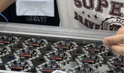
Insert the pins accurately according to the silkscreen mark to ensure that the components are completely fitted with the printed circuit boards without tilting.
Large-sized components are inserted first, and sensitive components are operated last.
2) Automatic Plug-in (suitable for large quantities)
Programming and controlling the plug-in machine to complete the high-speed insertion of standard parts (resistors/capacitors).
3) Temporary Fixation
Use special fixtures or high-temperature tape to temporarily fix the DIP plug-in on the PCB board to prevent displacement during welding, especially for special-shaped components.
2.3 Soldering Process
1) Wave Soldering (mainstream process)
Preheating: 100- Activate the flux at 150℃ to reduce thermal shock (helps the solder flow better and form a good bond with the pad).
Welding: tin bath temperature 230-260℃, control the wave peak height to cover 2/3 of the pins.
Cooling: forced air cooling to solidify the solder joints.
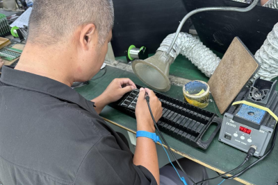
2) Manual Soldering (re-soldering/special components)
“Five-step Method”: heating the pad and pin → adding tin → melting tin and soaking → removing the tin wire → removing the soldering iron
Solder Joint Standard: conical, bright surface without burrs, no false solder joints/bridges.
2.4 Post-processing and Inspection
1) Pin Cutting
Specialized pin-cutting machine cuts off excess pins (≥1mm from the top of the solder joint).
2) Cleaning
Ultrasonic or solvent cleaning to remove flux residues.
3) Quality Inspection
Visual Inspection/AOI: Solder joint integrity, short circuit, and offset.
X-ray: Hidden solder joints and internal inspection of high-density boards.
Functional Test: Power on to verify electrical performance
2.5 Key Control Points
Temperature Management: The temperature difference between the wave soldering preheating zone and the soldering zone is ≤100℃ to prevent PCB delamination.
Soldering Time: The pin contacts the tin wave for 3-5 seconds. Too short will result in cold soldering, and too long will damage the components.
Protective Measures: High-frequency/high-voltage boards need to be sprayed with conformal coating to enhance reliability.
Note: DIP post-soldering needs to be coordinated with the SMT process. Usually, SMT reflow soldering is completed before the DIP plug-in to avoid secondary high temperature affecting the patch components.
3.The Difference between SMT Patch and DIP Post-soldering
SMT has a high initial equipment investment, but the unit cost of mass production is low; DIP equipment cost is low, suitable for small batch and multi-variety orders, but the labor cost is high. Modern manufacturing often adopts a mixed process (SMT+DIP): first SMT precision components, then DIP plug-in high-power devices, combined with AOI inspection and wave soldering parameter optimization, taking into account efficiency and reliability (such as communication base stations and automotive electronics).
SMT Patch
Through solder paste printing → SMT machine mounting → reflow soldering to achieve surface mounting, directly soldering pinless/short pin components (such as chips, resistors) on the PCB surface, with an accuracy of up to micron level.
DIP Post-soldering
It is necessary to insert the plug-in components with long pins (such as electrolytic capacitors and transformers) into the PCB through-holes → wave soldering/manual soldering → cutting the pins and cleaning, relying on mechanical insertion and pin soldering.
SMT Patch VS DIP Post-soldering
| Comparison Dimensions | SMT Patch | DIP Post-soldering |
| Component Package | Surface Mount Device (SMD), pins at the bottom | Dual in-line Package (DIP), pins on both sides |
| Space Utilization | High-density layout, support for double-sided mounting, product miniaturization | Loose layout, occupying a large PCB area |
| Production Efficiency | High degree of automation (patch speed reaches hundreds of thousands of points/hour) | Low efficiency of plug-in link, relying on manual/semi-automation |
| Reliability | Good solder joint consistency, defect rate <0.1%, suitable for high-frequency circuits | High mechanical strength of pins, strong vibration resistance |
| Maintenance Difficulty | Bottom pins are difficult to repair | Side pins are easy to replace and repair |
| Applicable Components | Micro components (01005 precision chips, etc.) | Large size/high power components (transformers, relays, etc.) |
| Application Scenarios | Consumer electronics (mobile phones, wearable devices), communication equipment, and other fields with high requirements for miniaturization and lightweight | Industrial control equipment, power modules, automotive electronics, and other scenes that need to withstand mechanical stress or high power |
4.Points that Need Special Attention during DIP Post-soldering
The details that are easily overlooked in the DIP post-soldering process directly affect the welding quality and product reliability. The following links need to be focused on:
4.1 Control of Welding Parameters
1) Precise Temperature Control
It is recommended to control the lead-free solder at 260°C~280°C and the lead solder at 230°C~250°C. Too high temperature will damage components (such as capacitor burnout), and too low temperature will easily lead to cold soldering.
Sensitive components (such as LEDs and crystal oscillators) need to be protected by heat-insulating fixtures to avoid thermal damage.
2) Welding Time Management
The single-point manual soldering time is strictly controlled within 2~3 seconds, and the wave soldering contact time is recommended to be 3~5 seconds. Insufficient time is prone to cold soldering, and too long time will accelerate solder oxidation.
3) Solder Selection Specifications
It is forbidden to mix lead-free/lead solder to avoid chemical reactions that reduce the reliability of solder joints; expired or inferior solders must be discarded.
4.2 Components and PCB Processing
1) Pin and Tolerance Control
The length of the pin extending from the pad should be moderate. Too long will easily lead to a tin tip, and too short will easily cause cold soldering; the tolerance of the plug-in should match the positioning hole.
After cutting the pin, check the flatness of the pin to prevent cold soldering or poor contact.
2) Anti-oxidation and Cleaning
The oxidized (blackened) PCB pad needs to be wiped with alcohol, and the damp board needs to be pre-baked (baked at 120°C for 1 to 2 hours), otherwise, the welding will easily produce pores.
3) Special Position Protection
OSP holes and other areas prone to leakage need to ensure full coverage of flux to prevent bridging or pulling tips.
4.3 Process Protection and Operation
1) Static Electricity Protection
The operator must wear an anti-static ring to prevent static electricity from damaging sensitive components.
2) High-temperature Adhesive Application
Non-welding areas (such as gold fingers) need to be affixed with high-temperature adhesive tape to avoid plugging holes or tin slag residue after wave soldering.
3) Support and Anti-deformation
Large-sized components require mechanical support to prevent the pad from lifting; the width of the wave soldering rail needs to be adjusted so that the PCB can slide freely to avoid extrusion and deformation.
4.4 Post-welding Inspection and Rework
Solder Point Defect Inspection
Focus on inspecting defects such as bridges, pores, and solder wraps. For example: continuous soldering requires adjustment of flux dosage and track inclination; pores need to be checked for PCB moisture.
Functional Test Coverage
ICT (in-circuit test) or FCT (functional test) must be performed after soldering is completed to ensure that the electrical performance meets the standards.
5.DIP Post-solderingFAQs
The five common welding defects in the DIP post-soldering process: False soldering/empty soldering, continuous soldering (tin bridge), pores/pinholes, tin tips, and solder joint cracks.
Tin Breaking Treatment: Use an automatic tin breaking machine to drill holes on the surface of the solder wire to release the flux gas and reduce the internal pressure.
Preheating Control: Preheat the solder wire to 100℃ to reduce the bursting caused by sudden temperature changes.
Use Segmented Welding: First, complete the A-side plug-in wave soldering, and then use selective dip soldering to process the B-side high components to avoid mutual interference.
Minor Oxidation: clean with anhydrous ethanol;
Severe Oxidation: need to be repaired by chemical nickel plating (Ni≥3μm/Au≥0.05μm);
The damp PCB needs to be baked at 125℃ for 2 hours.
Immediate Measures: adjust the wave soldering chain speed to 0.8–1.5m/min, reduce the tin wave height to 1/2 of the board thickness, and remove the tin bath oxide.
Long-term Prevention: add tin stripping sheets during the design stage and optimize the pin spacing; the positioning accuracy of the QFP package needs to be ±0.05mm.
When the pin diameter is greater than 1.2mm, the preheating temperature needs to be increased to 130~150℃ to avoid cold welding; after welding, an X-ray inspection is required to check whether the through-hole filling rate is ≥85%.
6.Summary
The post-soldering of DIP plug-ins is an important link in the PCBA production process, which is directly related to the performance and reliability of the product. By deeply understanding the entire process of DIP plug-in post-soldering, we can better master this key technology and improve production efficiency and product quality.
Table of Contents

Get Your PCB Quote!


