
PCB Stackup Design Guide: Multilayer, 4-Layer & Flex
A good PCB stackup is essential for signal integrity, EMI/EMC compliance, and thermal management, directly impacting device performance and reliability.
Get Your PCB Quote!
Table of Contents
- 1. Isingeniso: Umakhi Ongabonakali Wezogesi
- 2. Yini i-PCB Stackup? Ukudiliza Izendlalelo
- 3. Kungani I-PCB Stackup Ibalulekile: Izinsika Zokusebenza
- 4. I-Anatomy Yesitaki Se-PCB: Izinto Ezibalulekile Nezendlalelo
- 5. Izilungiselelo Ezijwayelekile Zesitaki se-PCB
- 6. Ukucatshangelwa Okubalulekile Kwedizayini Yesitaki Sesendlalelo Se-PCB Esilungile
- 7. Amasu Okunqwabelanisa Athuthukile kanye namathrendi esikhathi esizayo
- 8. Isiphetho: Ukuba Ngompetha Izendlalelo Zomklamo Ophakeme
- I-9. PCB isitaki Imibuzo Evame Ukubuzwas
- 10. Isifinyezo
1. Introduction: The Unseen Architect of Electronics
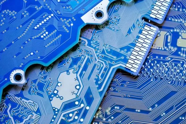
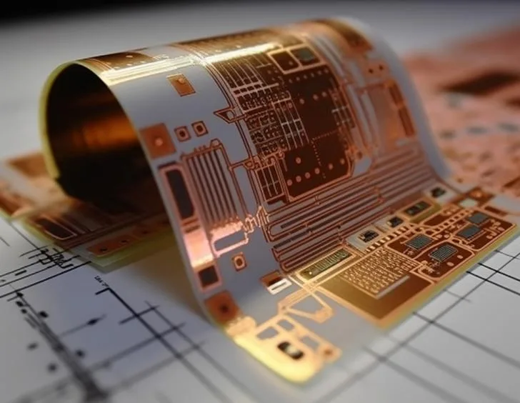
In the intricate world of electronics, where devices are shrinking and performance demands are soaring, the humble Printed Circuit Board (PCB) remains the bedrock. But beneath the green façade and visible traces lies a hidden architecture that dictates everything from signal speed to device reliability: the PCB stackup. Often underestimated, the stackup is the carefully arranged sequence of copper and insulating layers that form the backbone of any electronic product. It’s not just about connecting components; it’s about controlling electromagnetic interference (EMI), ensuring signal integrity, managing heat, and delivering clean power.
Imagine a skyscraper where each floor serves a specific purpose, and their arrangement directly impacts the building’s stability, safety, and functionality. A PCB stackup operates on a similar principle. A poorly designed stackup can lead to frustrating signal loss , unpredictable electromagnetic radiation, and even device failure, regardless of how perfectly the components are placed. Conversely, a well-optimized pcb layer stackup can transform a complex design into a robust, high-performance system.
This comprehensive guide will demystify the world of PCB stackups, exploring their critical importance, the various configurations from the standard 4-layer to advanced multilayer and flex pcb stackup designs, and the key considerations for achieving optimal performance. Whether you’re a seasoned engineer or an aspiring hobbyist, understanding PCB stackup is a non-negotiable step toward crafting cutting-edge electronic devices.
2. What is a PCB Stackup? Deconstructing the Layers
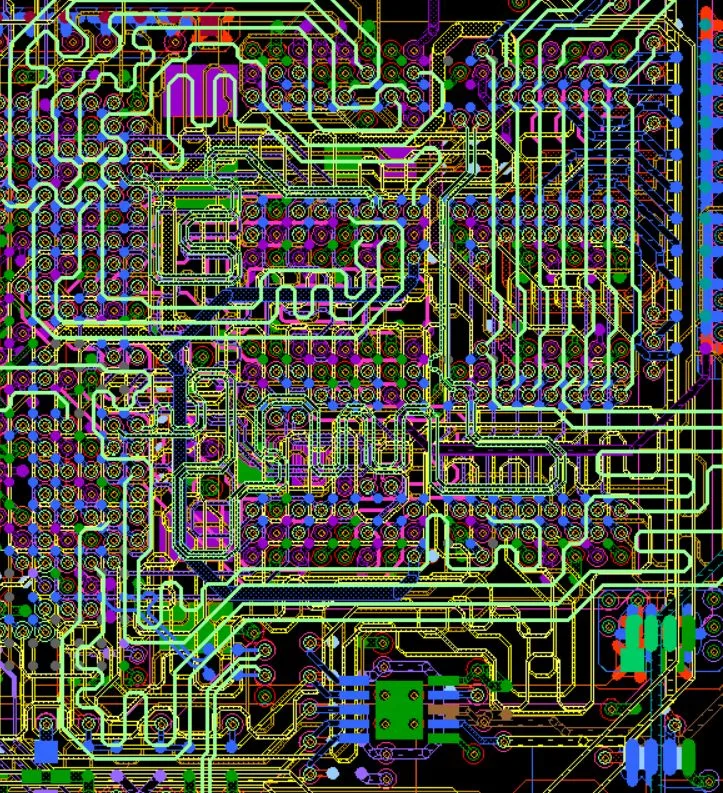
At its core, a pcb stackup refers to the arrangement of copper layers and insulating dielectric materials that make up a Printed Circuit Board. It’s essentially a cross-sectional view of the PCB, revealing how different layers are positioned relative to each other.
A typical PCB is not a monolithic block of material but rather a carefully laminated structure. These layers consist of:
1) Copper Foils: These are the conductive layers where traces (the “wires” on a PCB) are etched to connect components, and where power and ground planes are established.
2) Dielectric Materials: These are non-conductive, insulating layers that separate the copper layers. They prevent short circuits and play a crucial role in controlling impedance and signal propagation. Dielectric materials come in two main forms:
*Cores: These are rigid sheets of dielectric material with copper laminated onto both sides. They form the stable foundation of the stack up.
*Prepregs: These are thin sheets of dielectric material (typically fiberglass impregnated with resin) that are used to bond core layers together during the lamination process. When heated and pressed, the resin flows and cures , forming a solid insulating layer.
The specific order, thickness, and material properties of these layers collectively define the stackup. For instance, a standard 4 layer pcb stackup might consist of: Top Signal Layer, Ground Plane , Power Plane, Bottom Signal Layer, all separated by prepreg and core materials. The arrangement is not arbitrary; it’s a strategic design choice made to meet specific electrical and mechanical requirements.
3. Why PCB Stackup Matters: The Pillars of Performance
The design of a PCB stackup is far more than a manufacturing detail; it’s a fundamental aspect of electrical engineering that profoundly impacts a circuit’s performance. Neglecting proper stackup design can lead to a host of problems, from intermittent failures to complete system malfunction. Here’s why it’s so critical:
3.1. Signal Integrity: Keeping Signals Clean
High-speed digital signals are highly susceptible to noise, crosstalk, and impedance mismatches. A well-designed stackup provides clear return paths for signals, reducing parasitic inductance and capacitance. “Proper stackup design minimizes signal reflection and transmission line effects, which are critical for maintaining the integrity of high-speed digital and RF signals,” notes an article from Altium. By placing ground planes adjacent to signal layers, the stackup helps contain electromagnetic fields, preventing signals from radiating or interfering with adjacent traces.
3.2. Electromagnetic Compatibility (EMC): Taming the Noise
EMC refers to a device’s ability to function correctly in its electromagnetic environment without introducing intolerable electromagnetic disturbances to other devices. A robust stackup is crucial for EMI/EMC compliance. Continuous ground and power planes act as shields, containing electromagnetic energy within the board and preventing it from radiating outwards (emissions) or being absorbed from external sources (susceptibility). Poor stackup choices can lead to notorious EMI issues, causing designs to fail compliance testing.
3.3. Power Delivery Networks (PDN): Fueling the Circuit
Modern integrated circuits require stable and clean power. The stackup facilitates an efficient Power Delivery Network (PDN) by providing low-imped ance paths for power distribution. Dedicated power and ground planes, strategically placed close to each other, create a decoupling capacitance that helps filter out noise and supply stable voltage to components, especially during high-current switching events. This minimizes ground bounce and voltage fluctuations, which can otherwise cause logic errors.
3.4. Thermal Management: Staying Cool Under Pressure
As electronic components consume power, they generate heat. While thermal vias and heatsinks are primary thermal management tools, the PCB stack up indirectly plays a role. Copper planes can act as thermal conduits, helping to dissipate heat away from critical components. In power electronics, thicker copper layers in the stackup can significantly improve thermal dissipation capabilities.
3.5.Impedance Control: The Highway for High-Speed Signals
For high-frequency signals, traces behave as transmission lines, and their characteristic impedance must be precisely controlled. The stackup dictates this impedance through the width of the traces, the thickness of the dielectric materials, and the dielectric constant (Er) of those materials. Matching the trace impedance to the source and load impedances (typically 50 ohms for single-ended signals and 100 ohms for differential pairs) is vital to prevent reflections that degrade signal quality and reduce effective signal speeds.
3.6. Manufacturing Costs and Reliability
While more layers often mean higher manufacturing costs, an optimized stackup can prevent costly redesigns and re-spins due to performance issues. A well-thought-out multilayer pcb stackup can also lead to a more compact board size, reducing material costs. Furthermore, correct material selection and layer arrangement contribute to the mechanical robustness and long-term reliability of the PCB.
4. The Anatomy of a PCB Stackup: Materials and Layers
Understanding the individual components that make up a PCB stackup is essential for effective design. Each material plays a specific role in the board’s electrical and mechanical performance.
4.1. Core: The Foundation
Cores are rigid laminate sheets, typically composed of woven fiberglass cloth impregnated with epoxy resin (FR-4 being the most common type). They come with copper foil already laminated to both their top and bottom surfaces. Cores provide structural integrity and a stable dielectric constant. Their thickness is precisely controlled by the manufacturer.
4.2. Prepreg: The Adhesive and Insulator
Prepreg (pre-im pregnated) is a sheet of fiberglass material that has been impregnated with resin, but not yet fully cured. During the lamination process, under heat and pressure, the resin in the prepreg softens, flows, and then cures, bonding the copper foil layers and core layers together. Prepreg layers also provide dielectric separation between signal layers and power/ground planes. Their thickness and dielectric constant are crucial for impedance control. Different types of prepreg exist, offering varying dielectric constants, glass transition temperatures (Tg), and thicknesses.
4.3. Copper Foils: The Conductive Paths
These are the thin sheets of copper that form the conductive layers of the PCB. Traces are etched from these foils to create electrical connections between components. Copper foils are measured in ounces per square foot (oz/ft²), which corresponds to a specific thickness (e.g., 1 oz copper is approximately 1.37 mils or 35 micrometers thick ). Thicker copper is used for high-current applications or improved thermal dissipation.
4.4. Solder Mask and Silkscreen: Protection and Identification
While not part of the electrical stackup, these outer layers are crucial. Solder mask is a protective polymer layer applied over the copper traces to prevent solder bridges during assembly and protect the circuitry from environmental factors. Silkscreen is a non-conductive ink layer used to print component designators, logos, and other helpful information on the PCB surface.
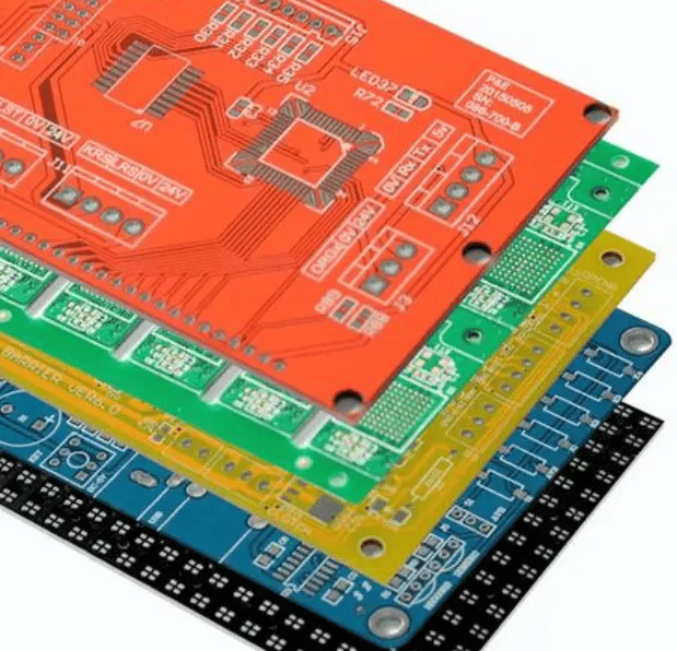
5. Common PCB Stackup Configurations
The choice of stackup configuration is one of the first and most important decisions in PCB design. It depends on the complexity of the circuit, frequency requirements, budget , and physical constraints.
5.1. The Basic Two-Layer Stackup
A two-layer PCB features copper on the top and bottom surfaces, separated by a single core layer.
* Configuration: Top Signal Layer / Core / Bottom Signal Layer
* Advantages: Lowest cost, simplest manufacturing.
* Limitations: Poor signal integrity (no dedicated ground plane for return paths), high EMI, difficult to route complex circuits, limited power distribution options.
* Use Cases: Simple, low-speed, low-frequency circuits where EMI is not a concern, such as basic hobby projects or power supply boards.
5.2. Standard 4 Layer PCB Stackup : The Workhorse of Modern Electronics
The standard 4 layer pcb stackup is arguably the most common multilayer configuration due to its excellent balance of cost, performance, and manufacturability. It offers significant advantages over two- layer boards for most modern electronic designs.
1) Common Configuration (Signal-Ground-Power-Signal):
Layer 1: Top Signal Layer
Layer 2: Ground Plane
Layer 3: Power Plane
Layer 4: Bottom Signal Layer
This is a popular choice because it provides clear return paths for signals on both outer layers by having adjacent ground and power planes. It also creates a good capacitance between the power and ground planes for decoupling.
2) Another Configuration (Signal-Ground-Ground-Signal):
Layer 1: Top Signal Layer
Layer 2: Ground Plane
Layer 3: Ground Plane
Layer 4: Bottom Signal Layer
This configuration offers superior EMI shielding by having two solid ground planes, but might require more effort for power distribution.
* Advantages:
Improved signal integrity (controlled impedance, clear return paths), reduced EMI, better power distribution, allows for more dense routing than 2-layer.
* Use Cases: Most digital and mixed-signal designs, embedded systems, consumer electronics, moderate-speed applications.
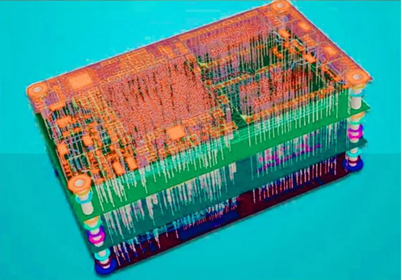
5.3. Multilayer PCB Stackup: Scaling Up for Complexity
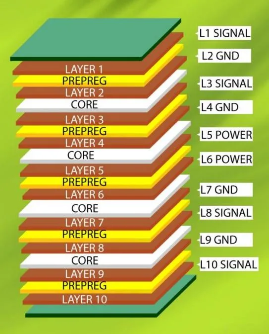
As designs become more complex, incorporating high-speed interfaces (DDR, PCIe, USB 3.0+ ), sensitive analog signals, and dense component counts, a simple 4-layer board might not suffice. Multilayer pcb stackup designs, with 6, 8, 10, or even more layers, offer greater flexibility and performance.
1) Common Principles:
* Pairing signal layers with adjacent ground planes to maintain controlled impedance and minimize crosstalk.
* Interleaving ground and power planes throughout the stack to improve PD N performance and shielding.
* Using multiple ground planes for different ground references (e.g., analog ground, digital ground) or to create isolated signal return paths.
* Burying high-speed signals between solid ground planes for maximum EMI containment.
2) Advantages: Superior signal integrity, excellent EMI/EMC performance, highly optimized PDN, very high component density, ability to isolate sensitive signals.
3) Limitations: Increased manufacturing cost , longer fabrication times, more complex design process.
4) Use Cases: High-performance computing, servers, data communications, RF circuits, advanced medical devices, aerospace electronics.
5.4. Flex PCB Stackup: Bending the Rules of Design
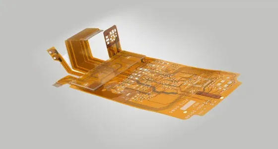
Flex pcb stackup designs present unique challenges and opportunities due to their ability to bend and conform to various shapes. The materials and construction differ significantly from rigid PCBs.
1) Materials: Instead of rigid FR-4 cores, flex PCBs use flexible dielectric materials like polyimide (PI) for both core and prepreg layers. Copper foils are typically thinner and more ductile.
2) Configuration: Can range from single -sided to multilayer flexible circuits. The stackup often incorporates adhesive layers (e.g., acrylic adhesives) to bond layers together, and coverlays (a flexible polymer film with an adhesive backing) to protect the outer copper traces.
3) Key Considerations:
* Bend Radius: The minimum radius to which a flex PCB can be bent without damaging the copper or dielectric. This is heavily influenced by the stackup thickness and material properties.
* Fat igue Life: Repeated bending can lead to material fatigue. Thinner, more ductile materials and symmetrical stackups improve fatigue life.
* Weight Reduction: Flex PCBs are inherently lighter than rigid boards.
* Thermal Management: Flexible materials generally have lower thermal conductivity than rigid FR-4.
4) Advantages: Space savings, weight reduction, dynamic bending (in some designs), simplified assembly (replaces cables and connectors).
5) Use Cases : Wearable electronics, medical implants, automotive sensors, cameras, smartphones, aerospace applications where weight and space are critical.
6. Key Design Considerations for an Optimal PCB Layer Stackup
Designing an effective pcb layer stack up involves careful consideration of several interconnected factors.
6.1. Layer Assignment and Routing Strategies
The strategic placement of signal, ground, and power layers is paramount.
* High-Speed Signals: Should ideally be routed on layers adjacent to solid ground planes to provide clear return paths and shield against EMI.
* Sensitive Analog Signals: Often benefit from dedicated ground planes and isolation from noisy digital signals.
* Critical Signal Types: Grouping signals by type (e.g., differential pairs, power, ground, high-speed) helps optimize layer allocation.
* Symmetry: For multilayer boards, a symmetrical stackup (e.g., 8-layer board where L1-L2 mirror L7-L8, and L3-L4 mirror L5-L6) can prevent board warp during manufacturing and improve structural integrity.
6.2. Dielectric Material Selection
The choice of core and prepreg materials significantly impacts electrical performance and manufacturing cost.
* Dielectric Constant (Er): A lower Er value allows for smaller trace widths for a given impedance, potentially leading to denser routing. However, it also means signals travel faster. Consistency in Er across layers is important for impedance control.
* Dissipation Factor (Df): Represents the signal loss within the dielectric material. For very high-frequency (GHz) applications, low -loss materials (with very low Df) are essential to minimize signal attenuation.
* Thermal Performance: Materials with higher glass transition temperatures (Tg) or better thermal conductivity might be chosen for high-power or high-temperature environments.
6.3. Via and Trace Design

Vias are vertical connections between layers. Proper via design, including selecting appropriate pad and drill sizes, is crucial. For high-speed signals, minimizing stub lengths on vias (by back-drilling or using blind/buried vias) reduces signal reflections. Trace width and spacing are also determined by impedance requirements and current carrying capacity.
6.4. Ground and Power Planes
Solid Planes: Prioritize solid ground and power planes over swiss-cheese designs (planes heavily fragmented by routing) to provide low-impedance paths, effective shielding, and stable voltage references.
Decoupling: Power and ground planes should be placed as close as possible to each other (e.g., 3-5 mils apart) to create a parallel plate capacitor, which provides intrinsic decoupling and helps filter noise at high frequencies.
Layer Transitions: Ensure consistent return paths when signals transition between layers. A signal changing from a top layer to a bottom layer via a through-hole must have a “return path via” to connect its reference ground plane on the top layer to the reference ground plane on the bottom layer .
7. Advanced Stackup Techniques and Future Trends

As electronics continue to evolve, so do stackup strategies. For extremely high-frequency applications, designers are increasingly utilizing specialized low-loss materials like Rogers laminates. Embedded passive components (resistors, capacitors) within the dielectric layers can reduce board size and improve performance by minimizing parasitic inductance. Furthermore, technologies like HDI (High-Density Interconnect) PCBs with microvias enable even denser routing and more compact designs, pushing the boundaries of what a PCB stackup can achieve. Software simulation tools are becoming indispensable for accurately modeling impedance, signal integrity, and EMI behavior before physical fabrication.
8. Conclusion: Mastering the Layers for Superior Design
The PCB stackup is much more than just a blueprint; it’s the fundamental architecture that dictates the electrical soul of an electronic product. From ensuring pristine signal integrity in high-speed digital circuits to managing thermal dissipation and maintaining EMI compliance, every layer and every material choice contributes significantly to the overall performance and reliability.
Whether you’re working with a standard 4 layer pcb stackup for a microcontroller board, designing a complex multilayer pcb stackup for a server , or navigating the unique challenges of a flex pcb stackup for a wearable device, a deep understanding of these principles is non-negotiable. By meticulously planning your pcb layer stackup, prioritizing clear return paths, controlling impedance, and selecting appropriate materials, you empower your designs to perform optimally, reduce development cycles, and ultimately deliver superior electronic products. Master the layers, and you master the art of modern PCB design.
9. PCB Stackup FAQs
A1: The primary purpose of a PCB stackup is to define the arrangement of conductive (copper) and insulating (dielectric) layers to optimize electrical performance (signal integrity, EMI /EMC, power delivery), mechanical strength, and thermal management, while considering manufacturing costs.
A2: A ground plane provides a stable reference voltage, offers a low-impedance return path for signals, acts as a shield against electromagnetic interference (EMI), and helps in heat dissipation. It’s crucial for maintaining signal integrity and reducing noise.
A3: A core is a rigid, fully cured laminate with copper foil already bonded to both sides, providing structural integrity. Prepreg is a partially cured, flexible fiberglass sheet that, when heated and pressed, flows and cures to bond core layers and copper foils together, acting as an adhesive and insulating layer.
A4: You should consider a multilayer PCB stackup (6 layers or more) when dealing with complex designs involving high-speed signals, dense component placement, sensitive analog circuitry, stringent EMI requirements, or the need for multiple power and ground planes for improved power delivery.
A5: Flex PCB stackups use flexible dielectric materials (like polyimide) instead of rigid FR-4. Unique considerations include bend radius, fatigue life for dynamic bending applications, thinner copper layers, and specialized protective layers (coverlays) to maintain flexibility and durability.
A6: The PCB stackup directly affects characteristic impedance by determining the trace width, the thickness of the dielectric material between a trace and its reference plane, and the dielectric constant (Er) of that material. Precise control over these factors is essential for matching impedance in high-speed designs.
A7: Ideally, power and ground planes should be placed as adjacent as possible, usually with a thin dielectric separation (e.g., 3-5 mils). This configuration creates an intrinsic parallel plate capacitance, enhancing power delivery network (PDN) decoupling and reducing ground bounce. They also serve as effective shielding layers.
A8: Absolutely. A poor stackup, especially one lacking continuous ground planes adjacent to signal layers or with fragmented power planes, can lead to uncontrolled electromagnetic fields, signal radiation, crosstalk, and overall increased electromagnetic interference (EMI), often causing a device to fail compliance testing.
10. Summary
The PCB stackup is a foundational aspect of electronic design, dictating the performance and reliability of any circuit board. It’s the strategic arrangement of conductive copper layers and insulating dielectric materials (cores and prepregs) that profoundly influences signal integrity, electromagnetic compatibility (EMC), power delivery, thermal management, and impedance control. From the simplicity of a 2-layer board to the complexity of advanced multilayer pcb stackup designs, each configuration offers specific advantages and challenges. The ubiquitous standard 4 layer pcb stackup provides a robust balance for most modern electronics, while specialized flex pcb stackup designs cater to unique form factors. Key design considerations include careful layer assignment, material selection based on dielectric constant and dissipation factor, and meticulous planning of power and ground planes to ensure clear signal return paths and stable power delivery. Mastering PCB stackup design is crucial for crafting high-performance, reliable, and compliant electronic products in today’s demanding technological landscape.
Table of Contents
- 1. Isingeniso: Umakhi Ongabonakali Wezogesi
- 2. Yini i-PCB Stackup? Ukudiliza Izendlalelo
- 3. Kungani I-PCB Stackup Ibalulekile: Izinsika Zokusebenza
- 4. I-Anatomy Yesitaki Se-PCB: Izinto Ezibalulekile Nezendlalelo
- 5. Izilungiselelo Ezijwayelekile Zesitaki se-PCB
- 6. Ukucatshangelwa Okubalulekile Kwedizayini Yesitaki Sesendlalelo Se-PCB Esilungile
- 7. Amasu Okunqwabelanisa Athuthukile kanye namathrendi esikhathi esizayo
- 8. Isiphetho: Ukuba Ngompetha Izendlalelo Zomklamo Ophakeme
- I-9. PCB isitaki Imibuzo Evame Ukubuzwas
- 10. Isifinyezo

Get Your PCB Quote!


