6 Steps to Printed Circuit Board Assembly Manufacturing
Get Your PCB Quote!

Assembly of printed circuit boards involves multiple steps that involve applying solder paste, placing components, inspecting, and testing. The best products can only be produced by following these procedures. The basic printed circuit board assembly steps are listed below:
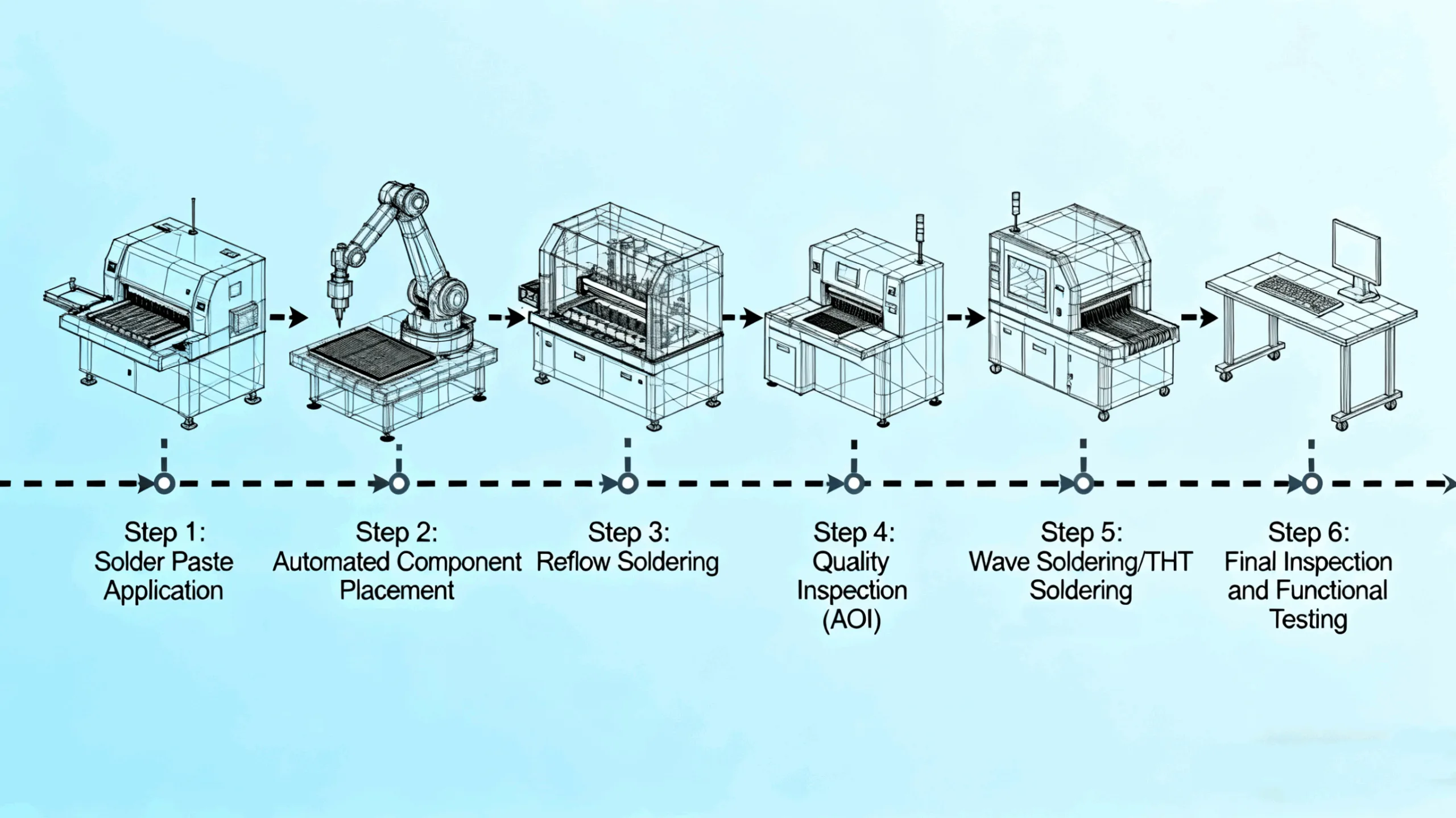
Step 1: Applying Solder Paste
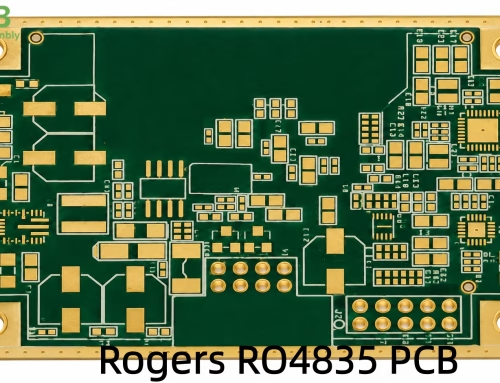
To begin the PCBA production process, the first step involves applying solder paste on a circuit board using a stencil. The PCBA manufacturer covers the circuit with solder paste. Silk-screening clothing is similar to the process in many ways. An alternative solution for PCB coverage is using a thin stainless-steel stencil instead. Solder paste consists of small metal balls composed of 96% Tin, 3% Silver, and 0.5% Copper. It is also lead-free.
Flux is a substance in solder paste that helps the solder melt and adhere to the surface, bonding with the solder. The right amount of paste must be used at the correct place. You can use different applicators to apply the paste in the right place. In an advanced PCBA production line, the PCB and soldering stencil are held in place by mechanical equipment. The manufacturer applies the solder paste to the desired area. The machine then evenly distributes the paste on the stencil, covering all the empty spaces. The solder paste will remain in the same place after the stencil has been removed.
Step 2: Automated Component Placement
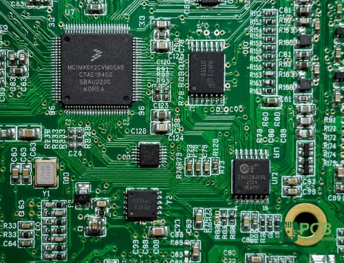
At this stage of the assembly process, the board with the solder paste added then enters the pick and place process. Automated machines are used during the pick and place process. Here, the manufacturer places the various SMD and electronic components onto the PCB. Most of the non-connector components on PCB today are SMD. Soldering SMD to the board surface is the next step in the PCBA process. The boards can be picked and assembled either automatically or manually. Traditionally, assemblers had to manually pick and place each component using tweezers to accomplish this task. However, PCB manufacturers now automate this process.
The main reason for this shift is that machines are generally more precise and reliable than humans. While humans are able to work quickly, fatigue and eyestrain usually start to set in after a few hours of handling such tiny components. Machines can run non-stop without getting tired. A vacuum gripper is used to pick up the PCB board. After positioning the PCB, the robot attaches the SMT on the PCB surface. The components are placed over the solder paste at the predetermined positions.
Step 3: Reflow Soldering
The third and final step in soldering involves reflow soldering. After components have been assembled and the solder paste applied, surface mount components must remain securely attached while waiting for it to harden before adhesion can take place between solder paste and board components. PCBA uses a procedure called “reflow” to achieve this. Printed circuit boards are placed onto a conveyor belt using a pick-and-place procedure and sent through a giant reflow oven that resembles commercial pizza ovens. Here, the boards are gradually heated to around 250 degrees Celsius (480 degrees Fahrenheit).
At this temperature, the solder paste will begin to disintegrate as its solder will melt. The PCB is then placed in the oven after the solder has melted. The molten solder is allowed to cool down and solidify by passing through a series of cooler heaters. The surface mount device (SMD), and the PCB, are permanently linked via solder joints. Especially for double-sided PCBA, several types of PCBA require special consideration during reflow. The stenciling and reflow of each side of the double-sided PCBA must be done separately. The stenciling, placement, and reflow of the side with the smallest and least amount of debris takes place before the other side.
Step 4: Inspection and Quality Control
After placing the components, the finished PCBA and assembled boards need to be tested for functionality and assembly capabilities. Movement during the reflow process often results in connections being lost completely or with poor-quality connections. This movement often leads to shortages, as misplaced components can sometimes connect circuit segments that should not be connected, creating errors. Inspecting is the process by which these defects are identified. Automated and manual inspection are options that can be employed.
These errors and displacements can be found using one of various inspection techniques. The three most popular inspection methods are X-ray, manual, and automated optical inspection. Automated optical inspection (AOI) is an ideal technique for high-volume PCBA assembly lines, and its machine is known as an automated optical inspection machine (AOI machine). It uses powerful cameras to “see” the PCB. The cameras are configured in different ways to be able to view the solder connections. AOI can detect lower-quality solder by comparing the way different solder connections reflect light. With its extremely fast processing speed, the AOI can process numerous PCBs in a short period.
Even with the growing trend towards automated manufacturing, PCBA still relies on manual inspection when processing small batches of PCBA. This means that manufacturers must perform visual inspections on-site after the reflow procedure. This method is an excellent way to guarantee the quality of circuit boards. However, as the number of boards inspected increases, this process becomes increasingly inefficient and unreliable. It is possible to become eye tired after looking at tiny components for more than an hour. This can reduce the accuracy of the inspection. X-rays are a different type of inspection technique.
This less popular inspection technique is most often used for more complex circuit cards or multi-layer boards. Using X-rays, an observer can see through the layers and visualize the lower layers to find any potential problems that may be hidden. These inspections can be performed frequently after the reflow process to look for any potential problems. This regular inspection ensures that problems are found and corrected as quickly as possible, helping manufacturers save time, labor, and resources.
Step 5: Through-Hole Component Insertion
Some boards may not contain SMD depending on the type of PCBA. PTH or plated-through-hole components are examples of. Plated through holes are holes in a PCB that are fully plated across the board. These holes allow PCB components to transmit signals from one side of the board. Solder paste will not adhere to the board in this situation because it will pass through the holes. During the final stages of PCB assembly PTH components will require more specialized techniques. In the manual soldering process, for example, each component is inserted by a single person at a station.
Step 6: Final Inspection and Functional Testing
The final and most critical stage of PCBA is testing, which indicates whether the process was successful or unsuccessful. Regular testing and inspection are vital throughout the assembly process for the same reasons that this testing is performed. The final inspection is performed after the PCBA soldering process has been completed. This test determines the functionality of the PCB. This evaluation is known as “functional testing.” This test simulates conditions under which the PCB would operate normally. The PCB is subjected to simulated signals and power during this test. Testers are also paying close attention to the electrical characteristics.
Summary
A printed circuit board assembly combines electronic components onto an intricate printed circuit board. This form of electronic device assembly is integral to our everyday lives. Testing a PCBA is an important step to ensure all components are placed correctly and function as intended. Various testing methods are employed to verify electrical connections and performance. The completed Printed Circuit Board Assembly is then ready to be integrated into larger electronic systems, powering devices ranging from consumer electronics to industrial machinery.