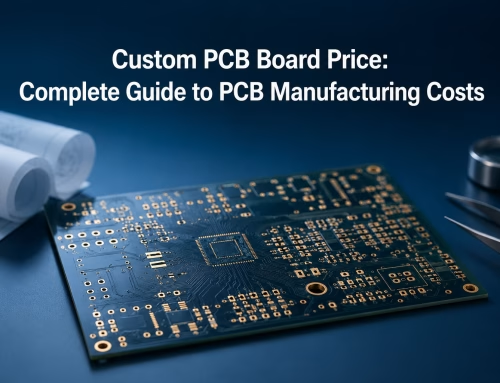
PCB Potting: Enhancing Reliability and Waterproofing
Among the waterproof PCB techniques, PCB potting is an important means of protecting components and circuits and improving board reliability and stability.
Get Your PCB Quote!
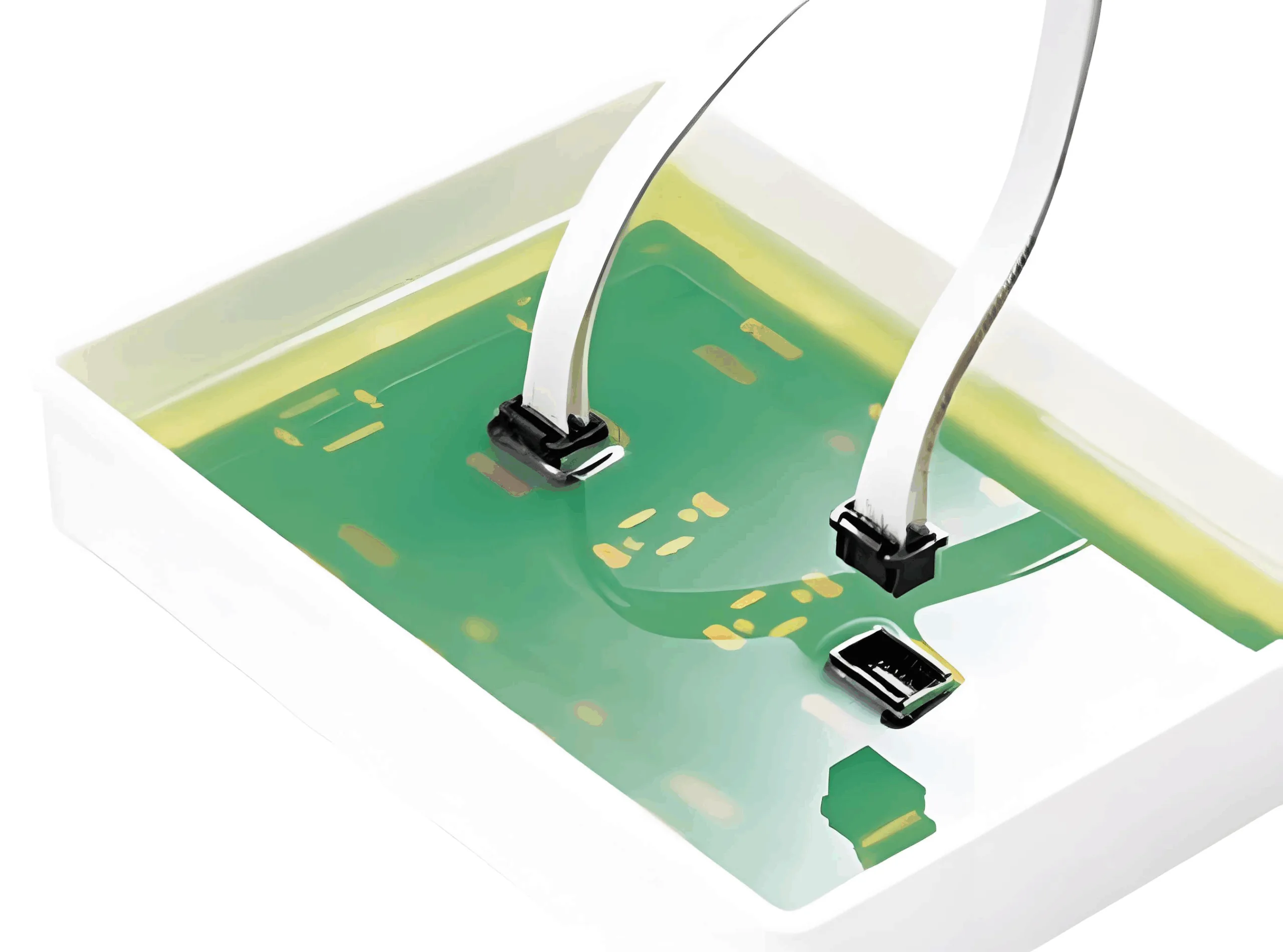
Table of Contents
Table of Contents
In the electronics field, waterproof PCB technique is a critical method for ensuring stable operation of electronic products in humid or underwater environments. Protecting printed circuit boards from damage is essential for guaranteeing the long-term reliability and stable performance of electronic devices. Among the common waterproof techniques, PCB potting involves encapsulating printed circuit boards within protective materials—typically resins or silicone compounds—to shield them from environmental hazards like moisture spray, dust, chemicals, and physical stress. This blog will delve into what PCB potting entails, why it matters, the processes involved, and its benefits in safeguarding electronics under challenging conditions.
1. What is PCB Potting?

PCB potting involves coating or injecting protective materials, such as silicone resin, epoxy resin or polyurethane, onto a PCB (printed circuit board). This process shields electronic components and circuits from moisture, dust, chemicals, and temperature fluctuations by encapsulating some or all of the exposed components and circuit traces on the board. The insulating material formed through curing enhances the integrity of electronic devices. It improves resistance to external impacts, vibrations and electromagnetic radiation, and boosts waterproofing, moisture resistance and dustproofing capabilities.
2. The Importance of Potting PCB
PCB potting is a critical waterproof process in electronics manufacturing, with its core purpose being to enhance the reliability and lifespan of circuit boards in complex environments by filling them with protective materials. Its primary functions are as follows:
1) Environmental Protection
Moisture and Water Resistance: Potting materials form a sealed layer that effectively blocks moisture, preventing circuit short-circuits or corrosion.
Dust and Chemical Corrosion Resistance: Potting circuit boards blocks dust, dirt, and corrosive substances, extending the lifespan of electronic devices in harsh environments.
2) Mechanical Protection
Impact and Vibration Resistance: Potted PCBs absorb mechanical stress, reducing the risk of component loosening or fracture due to vibration or shock—particularly suitable for aerospace and automotive electronics.
Enhancing Structural Integrity: Cured potting material strengthens the PCB’s physical structure, preventing direct component exposure.
3) Electrical and Thermal Management
Insulation Properties: PCB potting improves insulation between components and traces, preventing arcing in high-voltage applications and ensuring electronic equipment safety.
Thermal Management: Certain encapsulants (e.g., thermally conductive epoxy) aid heat transfer, preventing overheating damage to components and enhancing the board’s thermal stability.
3. Materials and Tools for PCB Potting
PCB potting is a critical process for protecting circuit boards and their components. By appropriately selecting potting materials and tools, the protective performance and reliability of PCBs can be effectively enhanced.
3.1 Common Potting Materials
1) Epoxy Resin Potting Compound

Features: High mechanical strength, excellent adhesion, superior electrical insulation, chemical corrosion resistance. However, prone to cracking under thermal shock and difficult to repair.
Applications: Small to medium-sized components such as LED drivers and sensors requiring high strength and confidentiality.
2) Silicone Potting Compound
Characteristics: Withstands extreme temperatures (-60°C to 200°C), offers excellent flexibility and shock resistance, and is repairable, but exhibits weaker adhesion.
Applications: Automotive electronics, outdoor equipment, and other fields requiring temperature stability and shock resistance.
3) Polyurethane Potting Compound
Features: Excellent elasticity, impact resistance, and flowability; suitable for complex structural filling. However, it exhibits poor aging resistance and high-temperature tolerance.
Applications: Sealing applications requiring high flowability, such as new energy battery packs.
3.2 Primary Potting Tools and Equipment
1) Potting Machine
Function: Automated mixing, blending, and potting of various adhesives including epoxy resin and silicone.
Advantages: High precision (±2% error), three-axis gantry design enhances efficiency and quality.
2) Auxiliary Tools
Molds and Release Agents: Used for forming; fluoroplastic or silicone rubber molds may eliminate the need for release agents.
Compounding Tools: Putty knives, three-roll mills (used when compound volume exceeds 250g).
Syringes: Suitable for complex potting in small-opening deep cavities.
3.3 Precautions
Adhesive Pre-Treatment: Stir thoroughly; heat the potting compound during winter to prevent sedimentation.
Equipment Calibration: Periodically inspect mixing accuracy and motion trajectories.
Defect Handling: If bubbles or tackiness appear after potting, rework the affected areas.
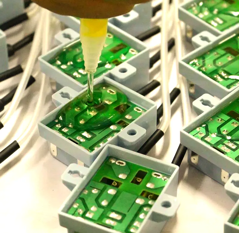
4. How to Pot A Circuit Board?
The PCB potting process requires meticulous attention to ensure complete coverage without damaging electronic components. Here are the detailed steps:
1) Preparation Phase
Clean the PCB: Ensure the board surface is free of dust, grease, and chemical residues to prevent compromising the encapsulant’s adhesion.
Preheat: Warm the PCB board to reduce the encapsulant’s viscosity and enhance its flowability.
Material Preparation: Weigh the potting compound (e.g., Part A and Part B) in the specified ratio and mix thoroughly.
2) Potting Process
Filling Method: Select injection molding, coating, or syringe encapsulation based on PCB structure. For complex shapes or deep holes, use a vacuum environment to prevent trapped air bubbles.
Curing: Allow the encapsulated board to cure undisturbed for 24 hours, or accelerate curing via heating (e.g., 70°C/24 hours or 100°C/8 hours).
3) Post-Processing and Testing
Excess Resin Removal: Scrape off excess resin from the surface to ensure smoothness.
Quality Inspection: Check for tackiness, bubbles, or defects after curing. Repair as necessary.
4) Key Considerations
Material Selection: Consider the encapsulant’s temperature resistance, adhesion, thermal expansion coefficient, etc., to suit different application environments.
Avoid Air Bubbles: Thoroughly clean and preheat components before encapsulation. For complex structures, design non-plated through holes (NPTH) to aid venting.
Safety Precautions: Ensure adequate ventilation during operation. Avoid skin contact and strictly follow material instructions.
5. Advantages and Disadvantages of Potting Process
PCB potting is a technique that provides protection by filling specific materials between electronic components and the circuit board. Its primary advantages and disadvantages are as follows:
5.1 Advantages of PCB Potting
Environmental Protection: Encapsulants effectively resist water, dust, and chemical corrosion, ensuring stable circuit board operation in harsh environments.
Mechanical Protection: Potted PCBs absorb vibration and shock, reducing component damage from mechanical stress.
Enhancing Electrical Performance: Potting can improve insulation of the circuit board, preventing short circuits or arcing—particularly beneficial for high-voltage applications.
Thermal Management: Certain materials (e.g., epoxy resins) possess thermal conductivity, aiding PCB heat dissipation.
Long-Term Stability: Silicone sealants exhibit strong weather resistance, enabling prolonged use between -50°C and 200°C without significant yellowing.
5.2 Disadvantages of PCB Potting
1) Repair Difficulty: Once potted, rework is challenging, especially with epoxy adhesives, which become nearly impossible to disassemble after curing.
2) Material Limitations:
Epoxy Resin: Poor resistance to thermal shock, prone to cracking, and high hardness may damage components.
Polyurethane Adhesive: Poor high-temperature resistance (<100°C), prone to bubbling and discoloration.
Silicone Adhesive: Weak bonding strength and low mechanical durability.
3) Complex Process: Some adhesives require vacuum degassing, with stringent curing conditions (e.g., precise temperature control).
4) High Cost: For silver paste potting processes, raw material expenses exceed 30% of total PCB manufacturing costs.
5.3 Comparison of Four Waterproof PCB Techniques
| Main Waterproof PCB Techniques | Advantages | Disadvantages |
| Conformal Coating | Low cost and undemanding operation requirements | The smell is too strong |
| Nano Coating | The process is simple, the coating is ultra-thin, and it can achieve 360° full protection, including connectors. | The high unit price is not conducive to reducing the cost of using large-area circuit boards. |
| Vacuum Coating | The coating has the highest uniformity and the strongest adhesion. | The equipment investment is high, and it places significant demands on the expertise and experience of the operators. |
| Potting Compound | PCB protection is the most reliable | Excessive glue usage and excessive thickness are detrimental to the design of thin and lightweight circuit boards. |
6. Common Issues and Solutions in PCB Potting

PCB potting is a critical process for protecting electronic components, but issues such as bubbles, cracks, and pinholes often arise during implementation. Below are common problems and their solutions:
6.1 Bubble Issues
Bubbles are the most common problem in potting, primarily caused by uneven mixing of the potting compound, changes in ambient temperature and humidity, or insufficient substrate surface cleanliness. Solutions include:
1) Select low-viscosity potting compounds with good flow properties (e.g., 8260N epoxy potting compound) to minimize air entrapment.
2) Use a diaphragm pump for application to avoid introducing bubbles from compressed air-driven paint cans.
3) Cure the compound: Allow the mixture to rest for 1 hour after mixing to let bubbles escape naturally.
4) Enhance substrate cleaning to ensure surfaces are free of moisture, dust, and other contaminants.
6.2 Cracking Issues
Cracks typically result from excessive coating thickness or residual flux. Primary solutions include:
1) Control coating thickness to prevent over-application.
2) Adjust the oven temperature profile to avoid excessive heat or rapid drying.
3) Thoroughly clean PCB boards, particularly around solder joints, to remove flux residues.
6.3 Pinhole Issues
Pinholes are primarily caused by improper spraying parameters (such as excessive air pressure or too close a distance) or substrate surface contamination. Solutions:
1) Optimize spraying equipment parameters, such as pressure, nozzle specifications, and spraying distance.
2) Control drying temperature within the range of 55–65°C to prevent rapid solvent evaporation due to high temperatures.
3) Ensure substrate surface cleanliness by removing moisture and dust.
6.4 Other Considerations
1) Material Selection: Potting materials must exhibit excellent adhesion, flexibility, heat resistance, chemical resistance, and weather resistance. Select epoxy resin (rigid, high insulation) or silicone rubber (elastic, superior temperature resistance) based on requirements. Epoxy resin has poor resistance to thermal cycling, while silicone rubber offers weaker adhesion but facilitates easier rework.
2) Environmental Control: Avoid extreme temperature and humidity fluctuations to prevent substrate deformation or metal oxidation.
3) Potting Thickness: Determine the encapsulation thickness based on the PCB’s actual requirements and operating environment. Typically, a thickness of 1-2mm is used. However, note that excessively thick layers may impair heat dissipation and signal transmission, while overly thin layers fail to provide adequate protection. Therefore, a comprehensive assessment based on specific conditions is necessary.
4) Process Flow: Prior to potting, the circuit board requires cleaning and pretreatment—such as removing dust, grease, and oxides—to ensure adhesion between the potting material and the board. During potting, parameters like temperature and pressure must be carefully controlled to guarantee material quality.
5) Potting Methods: Different encapsulation approaches—such as open-back, full-bottom encapsulation, or side encapsulation—can be selected based on specific requirements and components. Comprehensive consideration must be given to the post-encapsulation usage and mounting methods of the PCB.
By optimizing material selection, process parameters, and environmental management, PCB potting quality can be significantly enhanced.
7. PCB Potting FAQs
Potting is a protective process in which PCBs or electronic components are fully encapsulated in resin. This provides circuit boards with mechanical protection, environmental sealing and electrical insulation.
Filling an intended space with self-leveling materials is known as potting. This process is used among others to shield sensitive electronics from damaging outside influences or to provide camouflage or fire protection for components.
Potting and coating are two distinct protective techniques. Potting primarily involves filling, typically sealing the PCB entirely within resin to form a robust protective layer; whereas coating (such as conformal coating) focuses on surface application, resulting in a thinner layer (usually 50-90μm).
Currently, mainstream PCB potting materials are primarily categorized into three types: silicone resin potting compounds, epoxy resin potting compounds, and polyurethane potting compounds. Each possesses distinct characteristics and is suited for different application scenarios.
The terms “potting” and “encapsulation” are often used interchangeably, but technically, potting refers to a process where the shell or “pot” that is filled with resin becomes a part of the finished component. In encapsulation, the component and hardened resin are then removed from the pot to be placed in an assembly.
Difficulty in repair: Once cured, potting compounds are typically difficult to remove, especially epoxy and polyurethane potting compounds, which exhibit high hardness and strong adhesion. Repair often requires heating or mechanical removal, which can easily damage the PCB or components.
Clean the PCB board before potting (e.g., ultrasonic cleaning + high-pressure spraying) to remove surface grease and dust. Control the heating rate to prevent rapid surface curing of the potting compound, which traps internal air bubbles.
Assess uniformity by directly observing the compound’s color and texture. Consistent color without streaks or discoloration typically indicates adequate mixing. The mixture of two-component potting compounds should be uniform in colour. Localised colour variations suggest incomplete mixing.
8. Summary
Among the numerous waterproof PCB techniques, PCB potting serves as a critical method for protecting components and traces while enhancing board reliability. This process demands precise technical specifications and dimensional control across material selection, potting thickness, manufacturing procedures, and application methods. During PCB production and design, particular attention must be paid to potting requirements and precautions to ensure board quality and stability.

Get Quote Free