Tented vs. Untented Vias: Differences & How to Choose
“Untented Vias” and “Tented Vias” represent two distinct approaches that significantly impact both the performance of the PCB and its manufacturing costs.
Get Your PCB Quote!
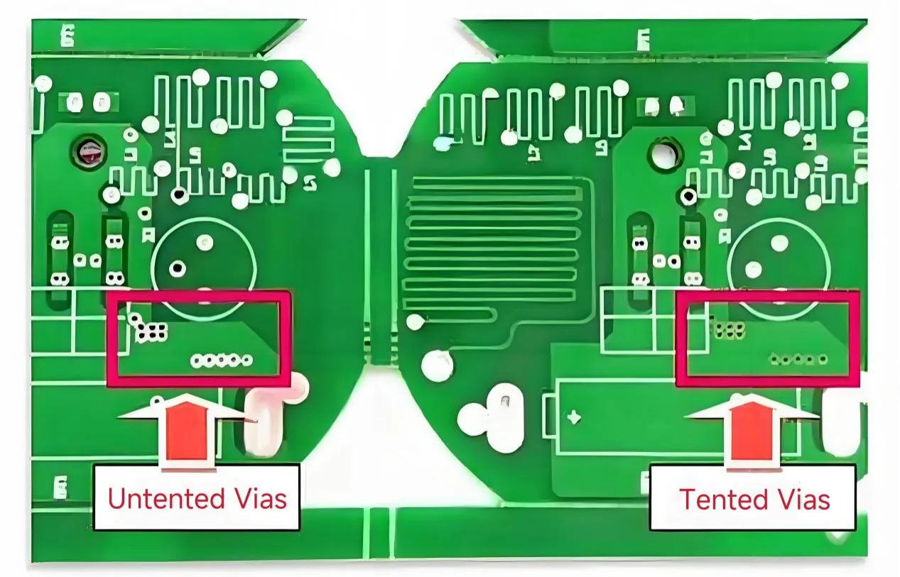
Table of Contents
“Tented Vias” and “Untented Vias” are two specialized terms in PCB design. If you’re new to electronics and hear someone say, “Design this PCB with untented vias,” you might think they’re an expert. But don’t be intimidated by the jargon—tented vias and untented vias simply refer to different methods of handling vias in PCB design. This article will thoroughly explain both via treatment methods, detailing their differences and application scenarios to help readers understand how to choose the appropriate via treatment based on specific requirements.
1. What are Untented Vias?
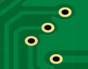
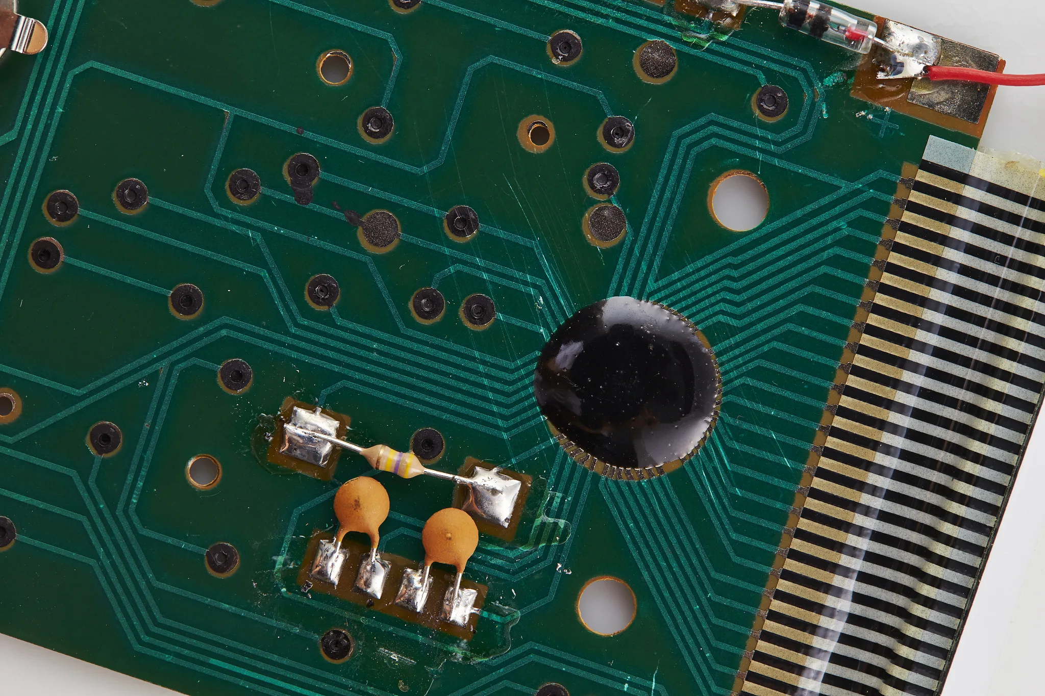
PCB untented vias refer to a process during PCB manufacturing where the solder mask (typically green ink) covering the top and bottom of a via is removed, fully exposing the copper wall or plated surface of the via.
1.1 What are the Purposes of Untented Vias?
Untented vias are typically created for specific design considerations:
1) Serving as Test Points
This is one of the most common reasons. The exposed copper ring serves as a test point during debugging, testing, or programming. Test probes can directly contact the copper surface for electrical measurements.
Engineers often need to check signals or power sources on specific networks when troubleshooting or testing boards. Untented vias provide easy access points. You don’t have to remove solder mask or look for other pads.
2) Enhancing Heat Dissipation
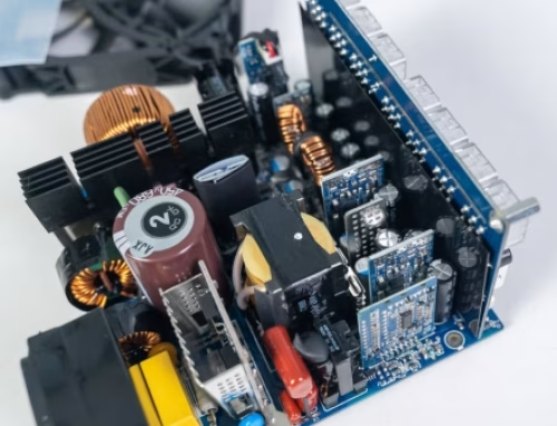
Some vias (particularly those connected to large copper pads or heat sinks) need thermal management. Removing the solder mask lets heat escape more easily through the exposed copper rings into the air. It also lets you add solder when needed to improve how well heat can flow. This practice is common in power supply designs and for dissipating heat from high-power components.
3) Increasing Current Carrying Capacity (Use with Caution)
For vias that need a higher current capacity, you can manually apply solder to the inner walls of these vias (via filling or solder plugging) during production or later problems. This increases the amount of copper in the via, reduces resistance, and improves its ability to carry electricity. Untented vias are a prerequisite for performing this solder filling operation.
Important Note: Untented vias alone provide little benefit for current carrying capacity. The critical factor is whether solder is applied after windowing. Untented vias may introduce other risks (see below).
4) Special Electrical Connections (Less Common)
In rare instances, special electrical connections may require the use of exposed via pads, such as soldering a short jumper wire or making contact with other conductive structures.
1.2 Considerations for Untented Vias (Risks and Drawbacks)
Although untented vias are sometimes necessary, they introduce potential issues and manufacturing/design challenges:
1) Increasing the Risk of Solder Bridging
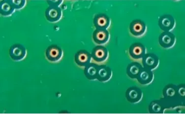
This is one of the most significant risks. After untenting, the exposed copper rings will solder like standard surface-mount pads during reflow or wave soldering. If the spacing between adjacent untented vias (or between a via and nearby traces/component pads) is too small, molten solder can easily form bridges (short circuits). These are harder to detect and repair than bridges between component leads.
Key Point: Ensure sufficient solder dam (the green mask gap between exposed copper) between untented vias and any other conductive structures (including other untented vias). Spacing requirements are typically stricter than for standard pads; consult your PCB manufacturer.
2) Causing Contamination and Oxidation
Copper that isn’t covered can get dirty or rusty more easily than copper that is covered by green oil. This can cause long-term reliability problems or affect the electrical connection during soldering or testing. The effect is especially noticeable when the product is not stored properly or in places with a lot of humidity and salt spray.
If the test point is intended for long-term use, surface oxidation resistance treatment is recommended (e.g., gold plating/ENIG, though ENIG may pose risks in micro-pores).
3) Affecting High-Frequency/High-Speed Signals
In high-speed digital circuits or high-frequency analog circuits, exposed pads may cause small problems with capacitance or inductance, or affect the continuity of impedance. Changes in the copper layer beneath untented areas (where the plane beneath the window is etched away from solder mask) may also affect the reference plane. This factor must be considered in extremely sensitive designs, though it usually doesn’t have a big impact.
4) Risk of Accidental Soldering (SMT Misidentification)
If the size and shape of a untented via resemble nearby component pads, there is a low probability that the SMT placement machine’s visual alignment system may misidentify it as a pad requiring placement (especially during production). Although the probability is low, it remains a consideration. Proper design can mitigate this risk (e.g., by employing significantly different dimensions or positions).
5) Affecting Aesthetics and Repairability
Exposed copper rings can affect the overall appearance of the circuit board. Solder beads nearby can be visually distracting during repair or debugging.
2. What are Tented Vias?
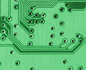
Via tenting is a process in PCB manufacturing where solder mask ink is applied to the surface of the solder ring around a via (plated-through hole). This creates an insulating protective layer. The “ink” in “Tented Vias” refers to the colored layer on the circuit board. For example, if your board is green, it means green ink was used; if your board is blue, it indicates blue ink was applied. “Untented Vias” refers to “not covering the solder mask ink.”
2.1 Advantages and Disadvantages of Via tenting
1) Basic Protective Functions
Oxidation Prevention: Solder resist ink covers surfaces, preventing air and moisture from reaching the copper layer. This keeps the copper layer from oxidizing and extends the lifespan of the circuit board.
Solder Overflow Prevention: This keeps solder paste from flowing into vias during soldering. This helps prevent short circuits and makes the product more reliable. It is particularly good for standard circuit boards.
Enhancing Mechanical Strength: Tented vias make PCB boards stronger. This makes them more resistant to bending and flexing. This reduces the risk of damage from external forces, such as vibration.
2) Cost and Process Advantages
Simple Process: You only need to apply solder mask ink to the surface of vias. This eliminates the need to fill the holes. As a result, the production workflow is faster.
Lower Cost: Tented vias are better than plugged vias because they use less material and cost less to make. This makes them a good choice for designs that need to be cost-effective.
3) Appearance and Applicability
Smooth Surface: After tenting, the PCB appears neat with no noticeable depressions, suitable for consumer electronics with modest aesthetic requirements.
Low-Frequency Circuit Compatibility: For standard electronic devices (e.g., home appliances, toys), tented vias sufficiently meet basic electrical performance needs.
4) Limitations
Affecting Heat Dissipation: If you cover holes with solder paste, it can make it harder for heat to move between the PCB and the heat sink. This can reduce the cooling efficiency.
Not Suitable for High-density Scenarios: Holes that aren’t filled can cause problems over time. In areas with a lot of small parts, like BGAs, you need to use[Via-in-Pad and Filled Vias] solder to fill the holes instead.
Affecting High-Frequency Signals: Unfilled vias may introduce parasitic capacitance or inductance; exercise caution in high-speed circuits.
5) Comparison Recommendations
Tented vs. Plugged: Prioritize tented vias for standard designs; employ plugged vias for high-reliability or high-frequency applications.
Design Specifications: Clearly mark via tenting requirements in Gerber files to ensure manufacturing consistency.
2.2 How does the Via Tenting Process Affect PCB Performance?
1) Affecting Electrical Performance
Signal Integrity: Variations in solder mask thickness can disrupt high-frequency signal transmission. For instance, a 10μm thickness deviation may cause ±3Ω fluctuations in the impedance of a 50Ω transmission line, resulting in up to 5dB differences in reflection loss at the 10GHz frequency band. In high-frequency scenarios (e.g., 5G base stations), uneven solder mask application may cause significant increases in signal bit error rates.
Insulation Protection: Tented vias prevent oxidation of via copper layers, avoids unintended electrical connections, and enhances insulation performance. However, bubbles introduced during the plugged vias process can become “killers” for high-frequency signals, generating noticeable reflections above 1GHz.
2) Affecting Mechanical Strength
Vibration and Impact Resistance: In industrial equipment, insufficient adhesion (<3N/cm) of the via tenting process may cause solder mask peeling, with a 15% failure rate after 1000 hours. Optimizing the curing process (e.g., increasing pencil hardness to 4H) can reduce maintenance-related damage rates by 70%.
Scratch Resistance: The cover coat must achieve a hardness of 3H or higher (IPC standard: 2H) to prevent tool scratches.
3) Affecting Thermal Management
Heat Dissipation and Thermal Stress: Uneven solder mask thickness may cause “via blowout” issues. For instance, a 30μm vs. 10μm thickness difference at via edges generates 12MPa stress during 260°C reflow soldering—exceeding the solder mask’s tensile strength (8MPa). Optimizing printing processes (e.g., controlling thickness deviation <5μm) reduces blowout rates from 5% to below 0.3%.
4) Cost and Process Selection
Cost-Effectiveness: Via tenting process is simple and low-cost, suitable for general electronics. However, high-frequency or high-reliability applications require balancing electrical performance and cost, potentially necessitating upgrades to plugged vias or epoxy-filled & capped vias.
2.3 Common Issues and Solutions
1) Uneven Solder Mask Coverage Causing Soldering Problems
Issue Manifestation: Uneven solder mask coverage may expose or completely seal vias, compromising soldering reliability.
Causes: Unstable solder mask application process (e.g., uneven thickness, trapped bubbles) or insufficient opening design.
Solutions: Optimize solder mask application process to ensure uniform coverage; verify solder mask dam design feasibility through DFM (Design for Manufacturability) checks.
2) Limited Thermal Performance
Issue Manifestation: Full solder mask coverage over vias may impede heat conduction through the vias, affecting heat dissipation for high-power components.
Cause: Solder mask exhibits poor thermal conductivity, and covered vias cannot directly participate in heat dissipation.
Solution: Implement a semi-tented design in critical thermal areas, or compensate for heat dissipation by increasing copper thickness.
3) Difficulties in Testing and Rework
Issue Manifestation: Fully covered tented vias cannot be directly tested via probes or reworked for soldering.
Cause: The solder mask layer blocks contact between the via and external tools.
Solution: Design untented vias near test points, or use laser windowing technology to locally expose the vias.
4) Oxidation Risk (Long-Term Reliability Issue)
Issue Manifestation: If the solder mask layer exhibits microcracks or process defects, copper inside vias may oxidize, leading to poor contact.
Cause: Incomplete solder mask protection allows moisture or contaminants to penetrate
Solution: Select high-reliability solder mask materials (e.g., LPI liquid photolithographic solder mask) and enhance process control.
5) High-Frequency Signal Interference
Issue Manifestation: High-frequency signals passing through Tented Vias may experience impedance mismatch due to changes in the solder mask dielectric constant.
Cause: Differences in dielectric constants between solder mask materials and air affect signal integrity.
Solution: Use low-dielectric-constant solder mask materials, or optimize via-surrounding trace design through simulation.
Common issues with tented vias often relate to solder mask processes, thermal management, testing, and signal integrity. Reliability can be significantly enhanced through design optimization (e.g., semi-tented, DFM checks) and material selection (e.g., high thermal conductivity solder mask).
3. The Difference Between Untented Vias and Via Tenting/Plugging
Untented Vias: The key point is that the solder mask layer is removed, exposing the copper ring. Whether the via hole itself is filled with resin or solder is a separate consideration (see below).
Tenting: Refers to completely covering the via pads and apertures with solder mask. This is the most common and safest standard treatment method. The interior of the apertures may be filled with resin or left unfilled (open).
Plugging: Refers to the process during manufacturing where resin (typically epoxy) or conductive material (such as copper paste) is used to fill the via holes. This prevents residual substances (like flux) from remaining inside the holes, enhances reliability, and prevents chemical solutions from infiltrating during subsequent processes.
Cap Plating/Via-in-Pad: Refers to the process where, after copper plating, the interior of the via hole is filled with electroplated copper and polished smooth through a specialized electroplating technique (sometimes combined with grinding). This enables the via to be used for soldering like a standard pad.
Key Relationships:
After via plugging (resin filling), options remain to apply tented vias (standard safety) or untented vias (for specific purposes).
Untented vias may be left empty or filled with resin (resin filling reduces voids and enhances reliability).
Untented vias without resin filling can be manually solder-filled when required.
4. PCB Via Design Recommendations
1) Default Tented Vias: Unless otherwise specified, prioritize via coverage with solder mask. This is the safest, most reliable, and least problematic standard practice.
2) Untented Vias Only for Specific Purposes: Only untenting on specific vias when there is a clear and necessary reason (e.g., designated test points, enhanced heat dissipation, planned manual solder filling). Avoid arbitrary untented vias.
3) Strictly Verify Clearance and Solder Mask Bridges: If you untent it, make sure you carefully check it to make sure there’s enough space between the untented vias and all the other conductive structures (like other pads, traces, and vias). This clearance typically requires a minimum equal to or greater than standard component pin spacing. Talk to the people who make your circuit boards to find out how thick the solder mask needs to be. Utilize DFM (Design for Manufacturability) tools for verification.
4) Clearly Communicate Intent to the Manufacturer: In Gerber files and manufacturing instructions, explicitly mark which vias require untenting and specify the purpose (e.g., for test points, solder filling). This enables the manufacturer to verify both design and process feasibility.
5) Weigh the Pros and Cons: Carefully balance the benefits of untented vias (ease of testing, enhanced thermal/current carrying capacity) against potential risks (bridging, oxidation).
In a word, untented via is a design option with specific applications that should be used cautiously. Avoid untenting unless absolutely necessary. If untenting is required, ensure sufficient clearance to mitigate short-circuit risks.
5. Tented and Untented Vias FAQs
1) What are tented vias?
A tented via is a via on a printed circuit board (PCB) that is covered with a layer of solder mask, which protects the exposed copper from corrosion, oxidation, and short circuits.
2) Are tented vias more expensive?
There is no doubt that tenting vias are a cost-effective method, it can provide protection to the vias and the copper around it. And tenting a via with liquid photoimageable solder mask is the most cost-effective method of tenting.
3) Why use tented vias?
A critical benefit of tenting vias in PCB assembly is that it prevents solder wicking, where molten solder paste is drawn into an untented via during reflow. This is especially problematic when vias are placed near surface mount pads, such as in BGA or via-in-pad designs.
4) Do tented vias affect heat dissipation?
Solder mask can slightly affect heat dissipation, but this can usually be compensated by increasing copper thickness or using thermal vias.
5) How can untented vias be avoided from shorting?
Strictly control the pad spacing and employ a solder mask dam design.
6) What are the common problems of tented vias?
Uneven solder mask coverage can easily lead to soldering issues.
Fully covered vias cannot be directly probed or reworked.
High-frequency signals passing through tented vias can cause impedance mismatch due to variations in the solder mask’s dielectric constant.
7) How can I optimize the solder mask coating process for tented vias?
Select a high-resolution liquid photoimageable solder mask (LPI) with heat resistance that meets the peak reflow temperature requirements (e.g., 245 ± 5°C) and a dielectric constant below 3.5 to reduce signal interference.
Control the solder mask thickness (typically 15-25μm). Too thick can lead to uneven via coverage, while too thin may not effectively prevent oxidation.
6. Summary
In the process of making printed circuit boards (PCBs), vias are important structures that connect circuits across different layers. There are different ways to make vias. Two of these are “untented vias” and “tented vias.” These two methods have a big impact on how well the circuit board works and how much it costs to make.

Get Quote Free