
PCB Etching Techniques: Everything You Should Know About It
PCB etching is a key process to selectively remove the non-circuit copper layer on the copper-clad board through chemical or physical methods.
Get Your PCB Quote!

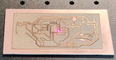
Take apart your electronic equipment. The motherboard is made up of densely packed lines that are as fine as spider silk. These lines can transmit high-speed signals stably. The birth of these fine lines is inseparable from the PCB etching process. It can be in the 5-micron-wide copper-clad board “carving,” which is equivalent to the diameter of a hair, 1/20. This allows cell phones, computers, and other equipment to be stuffed into increasingly small spaces with more features.
1. What is PCB Etching?

PCB etching is a core process in the manufacturing of printed circuit boards. Its basic concept can be summarized as follows: unwanted copper foils are selectively removed from copper-clad boards using chemical or physical methods, forming the predetermined circuit graphics.
1.1 Core Purpose: Forming Conductive Circuits
The core of PCB manufacturing is the formation of a precise network of copper conductors on an insulated substrate (e.g., FR-4) for connecting electronic components.
The starting material is a copper-clad laminate (CCL) covered with a uniform copper foil on one or two sides.
The goal of etching is to remove those areas of copper foil on the CCL that are not required to be wires, leaving only the designed lines, pads, and other conductive patterns.
1.2 Process Principle: Selective Protection and Dissolution
1) Graphics Transfer: Before etching, the graphics of the circuit design (Gerber file) need to be “copied” onto the copper side of the laminate by a photolithographic process. This usually involves:
Coating Resist: Coating the copper surface with a photosensitive resist (dry or wet film).
Exposure: Curing (negative process) or dissolving (positive process) the area of the copper foil to be retained (line pattern) by irradiating the resist with UV light through a negative (film) or direct imaging (LDI).
Develop: The uncured portion of the resist is washed away, exposing the area of copper foil underneath that needs to be etched away. The cured resist then adheres tightly to the copper foil to be retained, forming a protective layer.
2) Selective Etching: The developed copper-clad board is immersed (or sprayed) in an etching solution. The etching solution has the property of dissolving copper.
The area of the copper foil protected by the resist: the etching solution cannot dissolve it, and it is retained.
Areas of copper foil not protected by resist (exposed copper): are quickly dissolved by the etchant.
3) Removal of Resist (Descaling): After etching, the cured resist layer is stripped off, exposing the final copper circuit pattern. This layer serves as protection.
2. Different Types of Etching Techniques
PCB etching technology is the core link of circuit board manufacturing. According to the process, it can be divided into the following three categories, each with its own characteristics and application scenarios:
2.1 Wet Etching (Chemical Etching)
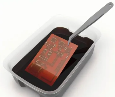
This is currently the most mainstream PCB etching method. A horizontal conveyor belt spray etching machine is usually used. The etching solution is sprayed evenly onto the board’s surface through nozzles to improve etching uniformity and efficiency.
1) Principle: Dissolve the unprotected copper layer with a chemical solution.
2) Commonly Used Etchant:
Acid Copper Chloride Etchant: Good stability, easy to regenerate (can be regenerated by chlorine or hydrogen peroxide oxidation), low cost, widely used. Reaction principle: 2CuCl₂ + Cu → 2CuCl + CuCl₂ (where CuCl dissolves copper).
Alkaline Copper Chloride Etchant: fast and stable etching rate, small side etching (high etching factor), especially suitable for fine circuit boards. The reaction principle depends on the formation of soluble complexes between copper and ammonia.
Persulfate Etchant: It is mainly used for single-panel applications or special occasions, such as gold plating after etching. It does not contain chlorine, but it is slightly less stable and more expensive..
Ferric Chloride Etchant: was the mainstream, but due to the difficulty in dealing with waste liquid, its tendency to precipitate, and the greater pollution, it has been less used for precision PCB production.
3) Process:
Copper-clad Plate Processing: single / double-sided copper-clad plate, hand-drawn with an oil-based pen or photolithography transfer printing circuit patterns as corrosion-resistant layer.
Corrosion Solution Configuration: commonly used hydrochloric acid (toilet bowl cleaner) and hydrogen peroxide mixture, or special etchant (such as a ferric chloride).
Etching Operation: The plate is immersed in the solution. The copper layer that is not covered by the ink undergoes an oxidation reaction. Shaking the container accelerates this reaction.
Cleaning and Stripping: Use banana water or plate washing water to remove the resist layer, exposing the copper line.
4) Characteristics: It is low-cost and simple to use, but has limited precision (line width greater than 0.2 mm) and creates pollution. Strict protection is needed (gloves, goggles, and ventilation).
2.2 Dry Etching (Plasma Etching)
1) Principle: The use of plasma in the active ions bombardment of the material surface to achieve selective etching.
2) Key Technology:
The vacuum reaction chamber passes into the etching gas (such as CF₄, Cl₂);
The gas is ionized by an RF electric field to form plasma.
Ions remove material from the exposed area by physical bombardment or chemical reaction.
3) Advantages:
Accuracy up to micron level, good sidewall perpendicularity;
Low damage, suitable for high-density integrated circuits;
No waste liquid pollution, process controllability;
4) Limitations: high cost of equipment, complex operation, mainly used for chips and other precision devices.
2.3 Laser Etching (Non-contact Processing)
1) Principle: High-energy laser beam directly vaporizes the copper layer without a chemical medium.
2) Mode of Operation:
CO₂/Fiber Laser: thermal effect ablation of the material (applies to metal layers).
UV Laser: photochemical cold working (reduction of heat-affected zone).
3) Innovative Features:
Environmentally Friendly: completely replaces chemical etching, eliminating acid and alkali waste liquid pollution.
High Efficiency: supports roll-to-roll continuous processing, width up to 2m×1.2m.
High Precision: CCD vision positioning realizes ±0.01mm alignment precision, with no burr.
Intelligent: fully automatic path programming, real-time temperature monitoring to prevent deformation.
4) Typical Applications: automotive heating film, flexible circuits, and other specialty PCBs.
2.4 Core Technology Comparison
| Type | Accuracy | Environmental Friendliness | Cost | Applicable Scenarios |
| Wet Etching | Low (>0.2mm) | Poor (chemical contamination) | Low | Experimental boards, simple circuits |
| Dry Etching | High (micron level) | Medium (gas control) | High | Chips, High-density ICs |
| Laser Etching | High (±0.01mm) | Excellent (zero contamination) | Medium-high | Specialty PCBs, high-volume production |
Laser etching is gradually replacing the traditional wet process due to both precision and environmental advantages, especially in automotive electronics, medical devices, and other fields to accelerate penetration. Dry etching is still an irreplaceable core technology for semiconductor micro-nano manufacturing.
3. The Application of Etching Technology
In electronic manufacturing, PCB etching technology plays the role of a “precision engraver.” The core of this technology involves the selective removal of excess copper layers on copper-clad board using chemical or physical methods to form circuit patterns. As electronic products become more miniaturized, high-frequency, and high-reliability, the etching process continues to expand its applications, mainly in the following areas:
3.1 Fine Line Manufacturing of High-precision Electronic Devices
1) Consumer Electronics Field
Mobile phone and computer motherboards are etched using a copper chloride solution in a process called wet etching. This method produces a minimum line width of 5 microns, which is equivalent to 1/20 of the diameter of a hair strand. This allows for high-density wiring. Optimizing the spraying system and additives controls side etching within 3 μm, guaranteeing stable signal transmission.
Smart wearable devices (e.g., bracelets) rely on ultra-fine line etching to ensure that miniature circuits realize complex functions in limited space.
2) 5G Communications and Chip Packaging
Dry etching (plasma bombardment) has become the first choice for high-frequency circuit boards (e.g., 5G base station antennas) and chip carrier boards due to its near-vertical etching angle and ±0.5μm error control capability. For example, carbon tetrafluoride plasma enables sub-micron circuits and enhances high-frequency signal integrity.
3.2 Thick Copper Etching Process for High Power Scenarios
Thick copper PCBs (copper thickness ≥ 3 oz) need to break through the etching uniformity challenge, mainly used in:
1) New Energy Vehicles: The battery management system (BMS) and motor controller use a thick copper layer of 4-12 ounces, allowing for a carrier flow that is up to four times that of an ordinary PCB. Pulse etching technology controls side etching of 3-ounce copper foil to within 8% by adjusting liquid injection parameters, thereby guaranteeing a minimum line width accuracy of 0.2 mm. At the same time, it reduces the temperature rise of the power module by 42%.
2) PV/Energy Storage System: Alkaline etching (sodium hydroxide solution) provides a smoother copper surface, reduces current loss, and increases inverter efficiency by more than 15%.
3.3 Customized Etching Solutions for Special Scenarios
1) Aerospace and Military
Plasma engraving technology is used to manufacture radiation-resistant circuit boards. Ion beam bombardment achieves etching without leaving behind chemical residue and prevents material degradation in space.
2) Medical Devices
Alkaline etching ensures smooth circuit surfaces for precision devices such as biosensors and reduces signal interference.
3) Flexible Printed Circuit Boards (FPC)
Plasma cleaning etches microporous adhesive residue. This solves the problem of submicron holes that are difficult to clean with chemical solutions. Plasma cleaning also enhances the reliability of flexible screens and other devices.
PCB etching technology is evolving from single corrosion to composite processing. Future applications in cutting-edge fields, such as quantum computing chips and three-dimensional packaging, will put its extreme precision and interdisciplinary synergy to the test.
4. Precautions for PCB Etching
To make high-precision lines, a good process alone is not enough. You have to control a few key factors to an extreme degree, just like when you’re baking a cake and have to control the temperature and time precisely.
4.1 Optimization of Etching Process Parameters
1) Etching Solution Selection and Proportioning
Acid Copper Chloride Etching Solution: For dry film/gold plating resist, the copper chloride concentration should be controlled at around 200 g/L (with a peak etching rate of 14.42 μm/min). The HCl concentration should not exceed 2.0 mol/L to prevent acid mist and equipment corrosion.
Alkaline Copper Chloride Etching Solution: The etching coefficient is higher (3.5-4). To reduce side corrosion, the pH level must be strictly lower than 8.5. To enhance edge flatness, the copper ion concentration should be maintained at 150 g/L or more.
Nitrate-based Etching Solution: minimize side-etching, can achieve near-vertical sidewalls, suitable for high-precision lines.
2) Temperature and Time Control
Temperature Range: The acidic liquid should be at a temperature of 50°C ± 2°C. The alkaline liquid should be above 46°C to accelerate the reaction. However, it must be used with an ammonia gas extraction system.
Etching Time: It is positively related to the copper thickness. For example, 1 oz of copper foil takes about 1.5 to 3 minutes. If it is too long, it leads to over-etching; if it is too short, there is a residual copper layer. The thinner the copper foil (e.g., 1/2 oz), the less side-etching occurs.
3) Equipment and Spraying Parameters
It adopts vertical spraying equipment with a spraying pressure of 0.2-0.3 MPa to ensure uniform coverage of the liquid. Horizontal equipment can easily cause over-etching.
The walking plate speed should match the etching rate (1 oz. copper foil is recommended at 1.5 to 2 m/min). The etching solution should be filtered two to three times per hour (with a precision of 0.2 μm).
4.2 Side-etching and edge control
1) Key Measures to Inhibit Side-etching
Etching Method: The spraying type reduces side-etching by more than 50% compared to the immersion type. The swinging nozzle design is preferred.
Design Optimization: The wires should be distributed uniformly, avoiding dense areas. Large areas of copper foil should be changed to a mesh structure to reduce uneven etching.
Copper Foil Selection: ultra-thin copper foil (≤1/2oz) significantly reduces side corrosion, suitable for fine lines (e.g., 0.0762mm line width).
2) Risks of Ridges (Shoulder Surges)
Excessive ridges can easily cause short circuits in the wires. This requires controlling the fluidity of the etchant and fluctuations in temperature (within ±1°C).
Alkaline etching solution can be added to the corrosion inhibitor to reduce lateral dissolution, enhancing the etching coefficient to 4.0 or more.
4.3 Material and Design Suitability
1) Substrate and Copper Foil Requirements
The crystalline structure and elongation of the copper foil affect etching uniformity. Therefore, it is recommended that high-purity electrolytic copper foils be used.
Thick copper foils (e.g., 2oz or more) need to reserve a larger line width/spacing margin to prevent etching deviations from leading to increased resistance or insulation failure.
2) Line Width/Spacing Design Rule
Copper foil thickness ↑ → minimum line width ↑ (Example: 1oz copper foil needs to be ≥0.1mm, 0.5oz can support 0.0762mm).
Impedance-sensitive lines require the calculation of etching deviation. The width error of high-speed signal lines should be controlled within ±10%.
4.4 Safety and Reprocessing
1) Operation Safety Specification
Protective Equipment: Wear acid-resistant gloves, goggles, and an anti-virus mask. Operate in a ventilated environment.
Waste Liquid Treatment: Copper-containing waste liquid must be neutralized and precipitated before discharge. Direct discharge is prohibited.
2) Cleaning and Drying
Selection of Plate Washing Water: Prioritize environmentally friendly water-based cleaning agent (concentration 2%-10%), together with ultrasonic cleaning (40kHz) to remove toner/resist layer.
Drying Process: DI water rinsing and hot air drying to prevent water stains from remaining.
4.5 Environment and Equipment Maintenance
1) Temperature and Humidity Control: The temperature of the etching area should be 22°C ± 1°C, and the humidity should be 40%-60% to prevent condensation. The photolithography area requires stricter precision (±0.1°C).
2) Etching Solution Regeneration: Regularly supplement with an oxidizing agent (such as sodium chlorate) to transform Cu⁺ to Cu²⁺. Replace 20% of the old liquid every eight hours to maintain activity.
5. PCB Etching FAQ
Chemically or physically removes the copper layer from the non-circuit areas of the PCB, leaving only the circuit graphics required for the design. The core of the process is to “carve” precision lines on the copper-clad board, with a minimum line width of 5 microns (about 1/20th of a hair).
Wet Etching: A chemical solution, such as copper chloride, can be used to dissolve the excess copper layer. This method is low-cost and high-efficiency (0.03 mm of copper foil can be etched in about three minutes). However, there is a side-etching problem with an error of about 20%.
Dry Etching: Using plasma bombardment on the copper layer results in minimal side-etching (±0.5 μm error), making it suitable for 5G base stations, chip packaging, and other high-precision applications. However, the cost of the equipment is high, and the process is slow.
Add corrosion inhibitor to wet etching to inhibit lateral corrosion;
Optimize the spray angle (30° fan spraying is recommended) to ensure uniform flushing of the liquid;
Dry etching controls the direction of vertical plasma bombardment by means of an electric field.
The resist layer is not completely removed (incomplete desmear);
The etching time is not enough, or the activity of the chemical solution decreases;
Uneven thickness of the electroplated copper layer leads to insufficient local protection.
Solution: Extend the etching time, replace the etching solution, and strengthen the quality inspection of the previous process.
Monitor the concentration of copper ions in the etching solution (high monovalent copper will reduce the rate);
Use an automatic PH control system to maintain the stability of the solution.
Uneven spray pressure due to clogged nozzles;
Drive rollers are not staggered to scratch the surface;
Insufficient liquid level in the equipment causes the pump to idle.
Problems such as uneven thickness of graphic plating and poor adhesion of dry film will be magnified in the etching stage, and need to be controlled from the developing and decoating process.
6. Summary
PCB etching is the use of photolithography to form a resist pattern as a “mask”, through chemical or physical methods, precise dissolution of the unprotected copper foil on the copper-clad board, so that the circuit design blueprints are transferred into the actual conductive copper wires of the precision manufacturing process. It is the bridge between the design drawings and the physical circuit board, and is the core reduction process of PCB manufacturing.

Get Your PCB Quote!


