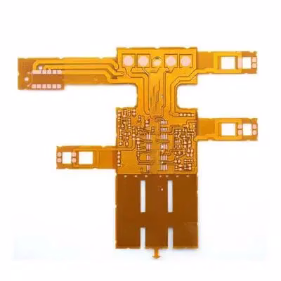
What is HDI PCB?
HDI stands for High Density Interconnector. A circuit board which has a higher wiring density per unit area as opposed to conventional board is called as HDI PCB. HDI PCBs have finer spaces and lines, minor vias and capture pads and higher connection pad density. It is helpful in enhancing electrical performance and reduction in weight and size of the equipment. HDI PCB is the better option for high-layer count and costly laminated boards.
The emergence of HDI technology has propelled the development of the PCB industry by enabling the integration of denser components like BGAs and QFPs.

HDI PCB Applications
HDI PCBs are predominantly used in high-end electronic devices such as communication equipment, computers, medical devices, and automobiles. Their high density, reliability, and superior performance make them critical in these applications.
Key HDI PCB Benefits
The evolution of high-density PCB technology has given engineers greater design freedom and flexibility than ever before. Designers using HDI high density interconnect methods now can place more components on both sides of the raw PCB if desired. In essence, an HDI PCB gives designers more space to work with, while allowing them to place smaller components even closer together. This means that a high-density interconnect PCB ultimately results in faster signal transmission along with enhanced signal quality.
HDI PCB is widely used to reduce the weight and overall dimensions of products, as well as to enhance the electrical performance of the device. The high-density PCB is regularly found in mobile phones, touch-screen devices, laptop computers, digital cameras and 4G network communications. The HDI PCB is also prominently featured in medical devices, as well as various electronic aircraft parts and components. The possibilities for high-density interconnect PCB technology seem almost limitless.
We’re capable of manufacturing HDI PCB up to 24 layers in various structures, check the following table for our available HDI PCB structures:
| HDI Structures |
Type of Micro vias |
Mass Production |
Small-Middle Batch |
Prototype | Available |
| 1+N+1 | Blind vias | Yes | Yes | Yes | 4 layers+ |
| 2+N+2 | Blind/Buried staggered vias |
Yes | Yes | Yes | 6 layers+ |
| 2+N+2 | Blind/Buried stacked vias |
Yes | Yes | Yes | 6 layers+ |
| 3+N+3 | Blind/Buried staggered vias |
/ | Yes | Yes | 8 layers+ |
| 3+N+3 | Blind/Buried stacked vias |
/ | / | Yes | 8 layers+ |
Check our HDI PCB capabilities by reviewing the table found below:
| Feature | Capability |
| Quality Grade | Standard IPC 2 |
| Number of Layers | 4 – 24layers |
| Order Quantity | 1pc – 10000+pcs |
| Build Time | 2days – 5weeks |
| Material | FR4 standard Tg 140°C,FR4 High Tg 170°C, FR4 and Rogers combined lamination |
| Board Size | Min 6*6mm | Max 457*610mm |
| Board Thickness | 0.4mm – 3.0mm |
| Copper Weight (Finished) | 0.5oz – 2.0oz |
| Min Tracing/Spacing | 2.5mil/2.5mil |
| Solder Mask Sides | As per the file |
| Solder Mask Color | Green, White, Blue, Black, Red, Yellow |
| Silkscreen Sides | As per the file |
| Silkscreen Color | White, Black, Yellow |
| Surface Finish | HASL – Hot Air Solder Leveling Lead Free HASL – RoHS ENIG – Electroless Nickle/Immersion Gold – RoHS Immersion Silver – RoHS Immersion Tin – RoHS OSP – Organic Solderability Preservatives – RoHS |
| Min Annular Ring | 4mil, 3mil – laser drill |
| Min Drilling Hole Diameter | 6mil, 4mil – laser drill |
| Max Exponents of Blind/Buried Vias | stacked vias for 3 layers interconnected, staggered vias for 4 layers interconnected |
| Other Techniques | Flex-rigid combination Via In Pad Buried Capacitor (only for Prototype PCB total area ≤1m²) |