
Thick Copper PCB

Contact Us

Contact us for all your PCB, PCBA, and custom service needs!

pcb

What Is Heavy Copper PCB?

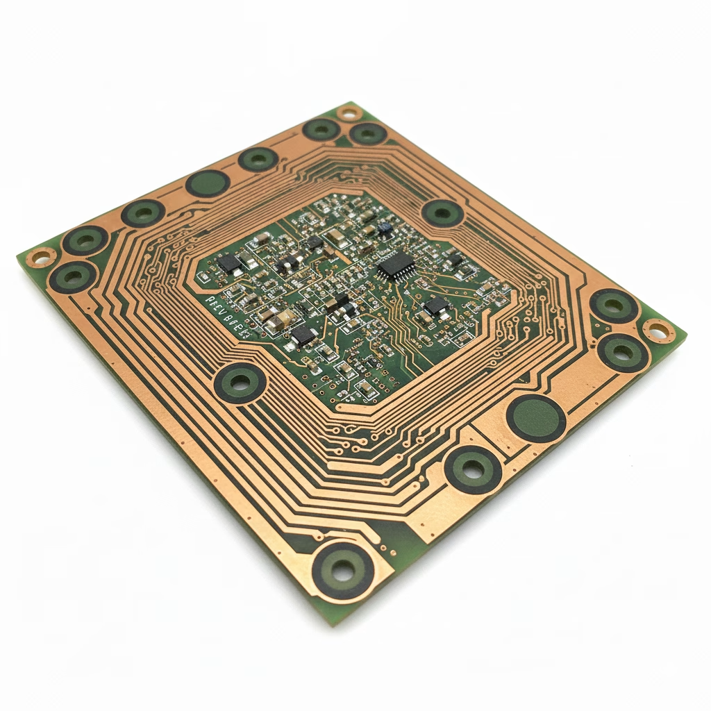
Heavy Copper PCB, as the name suggests, is a printed circuit board with thicker copper layers compared to standard PCBs. Typically, the copper layer thickness in standard PCBs ranges from 1oz to 2oz, while in Heavy Copper PCBs, the copper layer thickness can exceed 3oz. This technology provides improved current-carrying capacity and mechanical strength, making it widely used in high-voltage, high-current, and extreme environment electronic products.
Heavy Copper PCB

PCBAndAssembly is a globally trusted heavy copper PCB manufacturer with over 18 years of experience in multilayer circuit board fabrication. We specialize in thick copper PCBs that support high current flow, advanced thermal dissipation, and rugged mechanical reliability.

Our heavy copper PCB manufacturing capabilities include copper thickness up to 1000 μm (≈28 oz) on inner and outer layers, precision etching, and step plating for controlled layer buildup. We utilize advanced step plating and differential etching techniques to achieve these thick copper layers while maintaining clean edge profiles.

PCBAndAssembly manufactures heavy copper PCBs with finished copper weights up to 28 oz/ft² on outer layers and 28 oz/ft² on inner layers, enabling continuous current flow beyond 50 to 100 A, depending on conductor geometry.

Our minimum trace width and spacing for 12 oz high copper weights are 8 mil, adjusted based on etch factor modeling to mitigate undercut and maintain dimensional fidelity.

Copper circuits are patterned using dry film photolithography and controlled differential etching, ensuring consistent copper thickness across dense routing regions.

Heavy copper PCBs are engineered with high-Tg materials (≥170°C), including FR4-TG180+, ceramic-filled PTFE, and polyimide composites, to handle high current loads with minimal CTE mismatch. 

Thermal vias are deployed to route heat to copper planes or cold plates, supported by resin-coated or filled vias for mechanical stability. Our thermal modeling supports θJA reductions of up to 30% compared to standard PCBs. 

Prepreg stacks are selected to balance Z-axis expansion and dielectric constant, with thermal performance validated through thermal shock cycling (eg. -40°C to +125°C, 1,000+ cycles).

We support 2 to 16 layer builds with sequential lamination and via structures, including stacked microvias (4 to 6 mil laser), blind and buried vias, and via-in-pad with copper fill. 

Our plating achieves via wall copper thicknesses of ≥25 μm (1 mil), with aspect ratios up to 10:1 (eg. 0.008″ drill through 0.080″ board). 

All via structures are thermally stress-tested per IPC-TM-650 standards to verify reliability under thermal expansion forces.

Material selections include aluminum-core for high-wattage thermal paths, copper-core for direct bonded copper PCBs, and PTFE for RF impedance control (Dk ~2.2, Df < 0.0015). 

Standard FR4 (Tg130 to 180°C), polyimide, and ceramic substrates support diverse electrical, thermal, and mechanical demands. 

These substrates are laminated using prepregs matched for glass transition temperature and CTE, ensuring cohesive bonding during multiple lamination cycles.

Copper deposition is executed using step plating and pulse plating techniques to manage uniformity across complex geometries. 

In multi-thickness designs, deviation etching and panel-level thickness measurement (±10% tolerance) ensure consistent electrical characteristics. 

For inner layer thick copper routing, we implement dual-pass plating to mitigate overetching, with plating bath control at 24 to 26°C and current densities between 20 and 30 ASF.

Each heavy copper PCB undergoes optical resolution verification (AOI, 5 μm resolution), X-ray cross-sectioning of vias and internal layers, E-testing for continuity/isolation, and impedance testing for transmission line verification. 

Microsection analysis validates copper wall adhesion, plating thickness, and dielectric integrity, following IPC-6012 Class 2/3 performance classes.

Surface treatments include HASL (Sn63/Pb37, RoHS-compliant lead-free variants), ENIG (0.05 to 0.10 μm Au over 3 to 6 μm Ni), OSP, Immersion Tin (0.8 to 1.2 μm), Immersion Silver (0.15 to 0.35 μm), and ENEPIG. 

Surface finish is matched to final assembly method (eg. reflow vs. wave solder) and environmental exposure constraints, including sulfur resistance for outdoor electronics.

Production supports rapid prototyping (as short as 72 hours for ≤ 12-layer builds) and batch runs up to 10,000+ units. 

Each job includes full traceability (material lot, plating records, test logs), and is tracked under ISO 9001:2015 and IPC-A-610H standards. 

Statistical process control (SPC) ensures consistency in copper thickness, drill registration, and solder mask alignment across all builds.

Why Use Heavy Copper PCB?

Copper is a material with high electrical conductivity (58.5 MS/m) and low resistance (1.68 μΩ·cm).

Standard PCBs often fail under high-stress conditions. Engineers choose Heavy Copper primarily to bridge the gap between complex circuitry and extreme power demands.

Advantages of Heavy Copper PCB

Enhanced Reliability of Electronic Components

  • High Thermal and Electrical Conductivity: Heavy Copper PCBs offer excellent thermal and electrical conductivity, effectively dissipating and conducting heat to prevent component burnout due to heat concentration.
  • Applications: Suitable for power management systems, high-power LEDs, industrial control systems, and automotive electronics where high reliability is required.

Corrosion Resistance

  • Protective Layer: Heavy Copper PCBs can form a thin layer of copper oxide in the air, providing additional corrosion protection and extending the PCB’s service life.
  • Applications: Ideal for devices exposed to harsh environments, such as outdoor electrical equipment, marine equipment, and chemical equipment.

High Temperature Resistance and Thermal Stability

  • Stability: Heavy Copper PCBs maintain their physical and chemical properties in high-temperature environments and are not prone to decomposition or damage.
  • Applications: Suitable for applications in high-temperature environments, such as aerospace equipment, electric vehicle battery management systems, and high-power amplifiers.

Efficient Signal Transmission

  • Low Resistivity: Using Heavy Copper as the conductive layer provides low resistivity and excellent conductivity, enabling high-speed signal transmission and reducing signal loss.
  • Applications: Suitable for high-speed communication equipment, server motherboards, and high-frequency RF applications.

Electromagnetic Shielding

  • Superior Shielding Performance: Heavy Copper PCBs have excellent electromagnetic shielding capabilities. Their high conductivity allows them to effectively reflect and absorb electromagnetic waves, reducing electromagnetic interference (EMI).
  • Applications: Ideal for devices sensitive to electromagnetic interference, such as medical equipment, communication devices, and precision measurement instruments.

Machinability and High Mechanical Strength

  • Ease of Processing: Heavy Copper has good ductility and flexibility, making it easy to process into various shapes and sizes.
  • High Mechanical Strength: Heavy Copper PCBs provide sufficient mechanical strength, offering good physical protection and preventing damage during operation and use.
  • Applications: Suitable for applications requiring high mechanical strength and complex structures, such as military equipment, heavy machinery, and large industrial equipment.

What are the Design Considerations
for Heavy Copper PCBs?

Heavy copper PCB design demands precision across electrical, thermal, and mechanical domains due to the unique challenges presented by copper thicknesses ranging from 105 μm to 700 μm. Proper planning ensures reliability under high current loads and aggressive thermal cycling while maintaining manufacturability.

Trace Spacing and Width: Minimum spacing starts at 6 mils for 105 μm copper, increasing with thickness to avoid dielectric breakdown and shorting. For 210 μm copper, spacing may need to exceed 27 mils, with minimum trace widths of 12–25 mils based on the required current capacity and IPC-2221 guidelines.

Substrate Material and Thermal Stability: Select high-Tg base materials (>130°C) such as FR4-TG170+, PTFE, or ceramic for stability under thermal load. These materials must also exhibit low coefficients of thermal expansion (<17 ppm/°C) to prevent trace fracture or delamination from expansion mismatch during soldering and operation.

Copper Distribution and Fill Levels: Maintain even copper fill across layers to reduce mechanical stress and prevent Z-axis warping or void-induced delamination during press cycles. Use copper balancing techniques and avoid large open areas or highly localized trace clusters.

Prepreg and Laminate Selection: Use resin flow-optimized prepregs matched to copper volume to ensure void-free lamination and interlayer adhesion, especially in stackups with 6 oz+ copper. Simulation tools can assist in calculating optimal resin content and press cycle parameters.

Plating Process Control:Adjust galvanic plating parameters such as dwell time and current density to achieve uniform copper buildup on thick inner and outer layers. Step plating or pulse plating is recommended for builds with >4 oz copper per layer.

Solder Mask Application: Employ thick solder resist (>25 μm dry film) to reinforce mosaic edges, reduce flux ingress, and prevent mechanical erosion at the boundaries of copper features—especially critical on boards with high vibration exposure.

Thermal Path Optimization: Implement thermal vias, copper planes, and heat-spreading cores to manage ΔT under continuous current loads. Proper copper layer selection and thermal via density can significantly reduce junction-to-ambient thermal resistance.

Heavy Copper PCB Design Guidelines

Before finalizing a layout, match your baseline copper thickness to your application’s current and thermal requirements. These are reference values for spacing, path width, and material loss associated with different copper thicknesses.

Criteria 105 μm 140 μm 175 μm 210 μm
Loss (mils/mm) 3 / 0.08 5 / 0.13 6 / 0.15 7 / 0.18
Minimum Spacing (mils) 13 15 20 27
Minimum Trace Width (mils) 12 14 18 25

Copper PCB Manufacturing Capabilities Table

PCBAndAssembly is a highly skilled PCB manufacturer that can develop and produce a superior thick copper PCB product of the highest quality. We offer a thick copper PCB manufacturing service that uses copper weights of up to 15oz (525μm). Check our capabilities in the following table:

Feature Capability
Quality Grade Standard IPC 2
Number of Layers 2 – 24layers
Order Quantity 1pc – 10000+pcs
Build Time 2days – 5weeks
Material FR-4 Standard Tg 140°C, FR4-High Tg 170°C
Board Size Min 6mm x 6mm | Max 457mm x 610mm
Board Thickness 0.6mm – 6.5mm
Max Outer Layer Copper Weight (Finished) 15oz
Max Inner Layer Copper Weight 12oz
Min Tracing/Spacing For External layers:
4oz Cu 9mil/9mil
5oz Cu 11mil/11mil
6oz Cu 13mil/13mil
12oz Cu 20mil/32mil
15oz Cu 32mil/40milFor Internal layers:
4oz Cu 8mil/12mil
5oz Cu 10mil/14mil
6oz Cu 12mil/16mil
12oz Cu 20mil/32mil
Solder Mask Sides As per the file
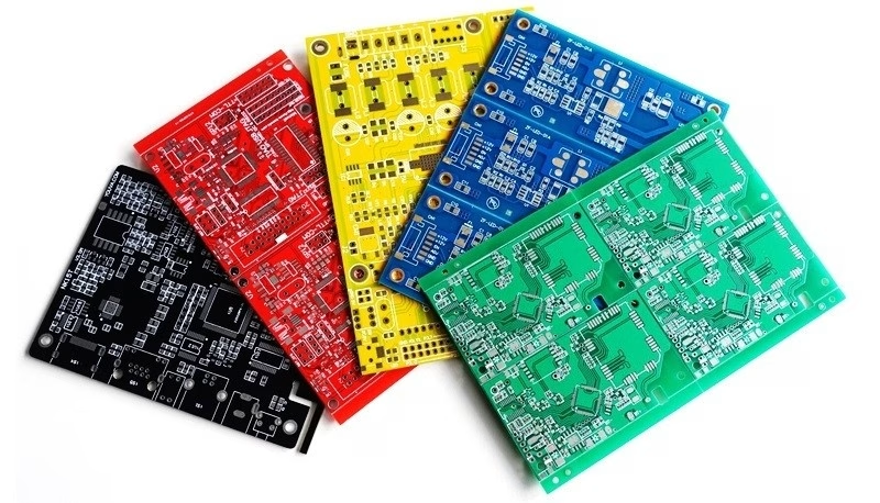
Solder Mask Color Green, White, Blue, Black, Red, Yellow
Silkscreen Sides As per the file
Silkscreen Color White, Black, Yellow
Surface Finish HASL – Hot Air Solder Leveling
Lead Free HASL – RoHS
ENIG – Electroless Nickle/Immersion Gold – RoHS
Min Annular Ring 6mil
Min Drilling Hole Diameter 10mil
Other Techniques Gold fingers
Blind/Buried Vias

Heavy Copper PCB FAQs

A standard PCB typically features 1 oz/ft² of copper, corresponding to a finished thickness of 35 μm (±10%). In some designs, especially for enhanced thermal or current-carrying needs, the finished copper may be increased to 2 oz/ft² (≈70 μm) through electroplating. This thickness applies to internal and external layers unless specified differently in the board stack-up.

Selecting the appropriate copper thickness depends on three primary parameters: 

  • Current-carrying requirement (Amps) 
  • Permissible temperature rise (°C) 
  • Trace width and layer type (inner vs. outer)

Use IPC-2221 guidelines or a copper thickness calculator to determine the required cross-sectional area. For example, a 5 mm wide trace on an outer layer with 105 μm copper can safely carry ~50 to 60 A with a 20°C temperature rise in free air. Consider using thicker copper (≥4 oz/ft²) when you need high power density, thermal stress, or mechanical reinforcement.

Base copper weight refers to the initial thickness of the copper foil laminated onto the PCB core or prepreg before any plating is performed. Common base copper weights are 0.5 oz, 1 oz, or 2 oz/ft², equivalent to 17.5 μm, 35 μm, or 70 μm, respectively. During fabrication, this base layer is thickened via electroplating, particularly in PTHs (plated through holes), to meet final design requirements.

Heavy copper PCBs, typically defined as PCBs with ≥3 oz/ft² copper per layer, offer several key advantages:

  • High current carrying capacity: Wide, thick copper traces reduce resistive losses and enable current flow >100 A in some designs. 
  • Improved heat dissipation: Greater copper mass lowers thermal resistance (θJA), helping to transfer heat to external heatsinks or thermal vias. 
  • Enhanced mechanical strength: Thick copper walls reinforce via barrels and connector pads, improving reliability under thermal cycling and vibration. 
  • System-level simplification: Supports power and control circuits on a single PCB, reducing wiring, interconnect losses, and overall footprint. 
  • Long-term durability: Withstands extreme temperature cycling and overload conditions better than standard copper PCBs.

Contact Us

Contact us for all your PCB, PCBA, and custom service needs!

pcb
