12 Layer PCB

12 Layer PCB Stack Up Manufacturers
12 layer PCB stack-up manufacturers produce complex circuit boards with multiple conductive layers. These boards are essential for high-density electronic devices that require advanced functionality. Manufacturers like PCBAndAssembly use specialized equipment and techniques to create precise layer alignments and connections.
The production process involves careful planning of the PCB stackup design. This includes determining the placement of signal layers, power planes, and ground planes. Manufacturers must also consider factors like impedance control and signal integrity. Quality control is crucial throughout the fabrication process to ensure the final product meets strict industry standards.
At PCBAndAssembly, we manufacture 12 layer PCBs for complex layouts, dense routing and stable performance across every layer.
Each 12 layer PCB stack is engineered in house, fabricated to IPC standards, and supported with complete assembly services.
Turnaround starts at 2 weeks for prototypes, with standard production in 4 to 5 weeks.
- HDI stack ups, via-in-pad, and X-ray tested builds
- Certified to ISO 9001, IATF 16949, and IPC-6012
- Controlled impedance with 3/3 mil trace/space routing
What Is a 12-Layer PCB?
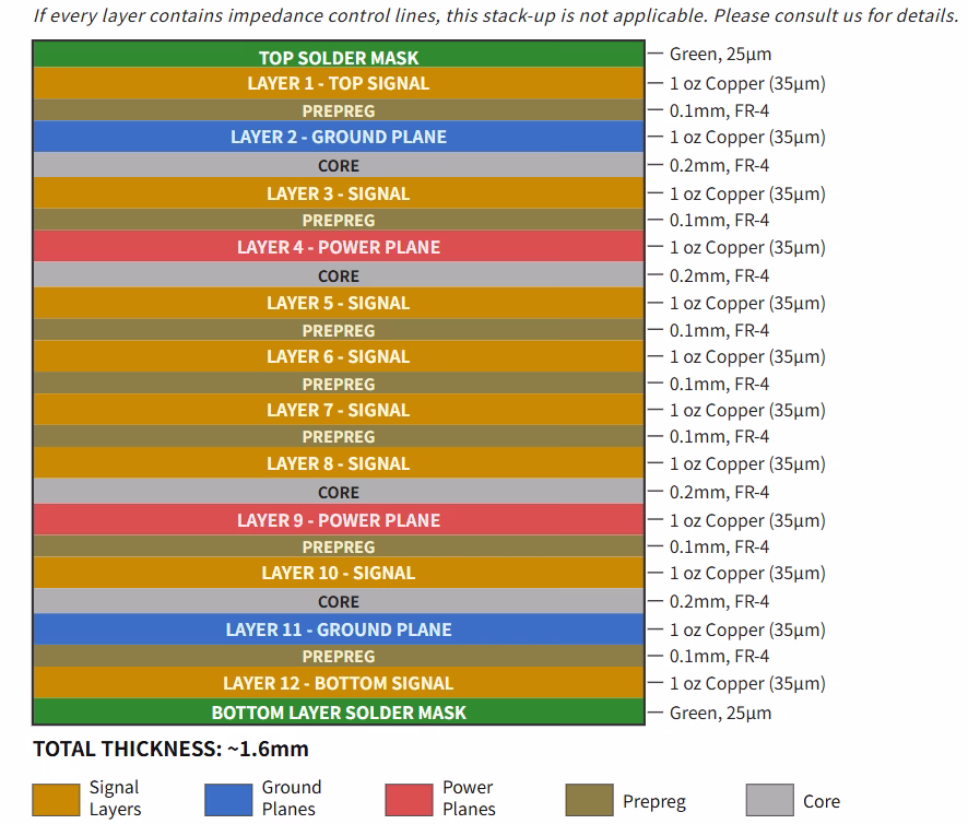
A 12-layer PCB is a type of multilayer board built from twelve stacked and laminated copper layers, separated by insulating dielectric material. These layers are arranged in a specific sequence called a 12 layer PCB stack up, which defines the position of signal layers, power planes, and ground layers.
The structure is chosen to support dense routing, impedance-controlled signals, and reliable power distribution without increasing the board’s physical footprint. Most designs use the outer layers for component routing, while inner layers manage cross-sheet signals, voltage rails and shielding.
Vias connect specific layers based on routing constraints, allowing data and power to move vertically through the board. The result is a layout that can support compact, high speed, and EMI-sensitive circuits in a format that balances electrical performance and mechanical stability. Choose a dedicated 12 layer PCB manufacturer for best results.
Why Choose a 12 Layer PCB Stackup?
Increased Circuit Density
- More layers allow for higher component density
- Enables miniaturization of electronic devices
Improved Signal Integrity
- Better control over electromagnetic interference
- Reduced crosstalk between signal traces
Enhanced Power Distribution
- Dedicated power and ground planes for stable voltage supply
- Improved thermal management in high-power applications
Design Flexibility
- More routing options for complex circuit layouts
- Ability to separate high-speed and low-speed signals
Our 12 Layer PCB Manufacturer Capabilities
| Material Category | Material Type | Properties | Uses / Applications |
| Substrate | FR-4 | Flame-retardant, good insulation, and cost-effective. | Standard 12-layer PCBs. |
| Rogers Materials | Low loss, controlled dielectric, high-frequency performance. | RF and microwave applications. | |
| Conductor | Copper Foil (0.5 to 2 oz) | Standard conductivity, various thicknesses. | Signal layers and power planes. |
| Bonding | Prepreg | Adhesive properties, dielectric insulation. | Layer bonding in the stack up. |
| Core Materials | Structural support, copper-clad. | Inner layer pairs. | |
| Finishing | ENIG (Ni/Au) | Excellent solderability, corrosion protection. | Surface mount pads. |
| HASL | Cost-effective, good solderability. | General purpose finish. | |
| Protection | Solder Mask | Electrical insulation, protection. | Circuit protection. |
| Silkscreen | Durable printing, component identification. | Assembly markings. |