
What are Metal Core PCB?
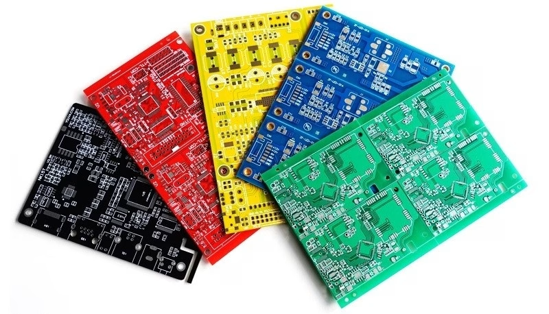
Metal Core PCBs (MCPCBs) are printed circuit boards with a metal base, typically aluminum or copper, for efficient heat dissipation. They improve thermal management, making them ideal for high-power and high-heat applications like LED lighting and power electronics. MCPCBs enhance performance and reliability by reducing heat buildup.
Core Materials
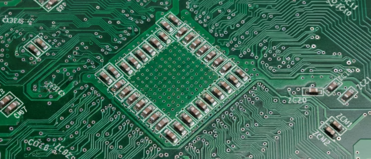
We offer copper, aluminium, copper-aluminium composite, stainless steel, and iron as metal core PCB materials, each selected based on thermal conductivity, mechanical strength, and chemical compatibility.
Aluminum is used in ~85% of MCPCB builds due to its conductivity range of 1.0 to 2.2 W/m·K and low density (2.7 g/cm³), making it ideal for metal core PCB LED and general-purpose thermal designs.
Copper cores offer conductivity up to 4.0 W/m·K with higher tensile strength (210 MPa+) and are deployed in high-power PCBs, such as inverter modules and EV subsystems.
Steel and iron cores are selected where increased rigidity and resistance to deformation under load are needed, such as in vibration-exposed assemblies.
Layer Structures
We fabricate single-layer, double-layer, and multilayer metal core PCBs using dielectric bonding and press lamination.
Single-sided MCPCBs consist of a copper trace layer, a thermally conductive dielectric, and a solid metal core optimized for vertical heat evacuation.
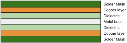
Double-sided builds use high thermal conductivity dielectric (≥2 W/m·K) on both sides of the metal substrate, allowing plated through-hole (PTH) connectivity for top/bottom side SMD assembly.
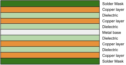
Multilayer MCPCBs use stacked copper and dielectric layers over the core, with blind/buried vias, ground/power planes, and isolation barriers, supporting high-frequency PCBs and high-density RF modules.
Thickness Range
We offer metal core thicknesses from 0.4 to 3.2mm, depending on the required mechanical rigidity and heat transfer mass.
Copper foil thickness ranges from 0.33 oz (12 μm) to 10 oz (350 μm), supporting trace widths from 0.15 mm with aspect ratios up to 10:1. Dielectric materials are applied in 50 to 125 μm layers using filled or unfilled resin systems with thermal conductivity from 1.0 to 15 W/m·K.
Minimum line/space resolution is 3 mil/3 mil with ±10% trace width tolerance after etching.
Manufacturing Process
Fabrication begins with DFM review and stack-up simulation, including thermal path modeling and expansion coefficient balancing.
Circuit imaging uses UV photoresist exposure in ISO Class 7 cleanrooms. Etching is performed with alkaline or acidic chemistries, depending on copper weight.
Mechanical or laser drilling enables via diameters down to 0.2 mm; for metal-backed PCBs, insulating collars are applied to prevent shorting.
ENIG, OSP, or HASL finishes are applied before full-panel AOI, flying probe, and impedance testing verify electrical performance.
Surface Finishing
We support industry-standard finishes including HASL (SnPb or lead-free), ENIG (Ni ≥120 μin, Au ≥2 μin), and OSP (ENTEK Plus HT).
Selective plating for high-wear pads and edge contacts is available on request. All finishes are RoHS compliant and conform to IPC-4552/4553 standards.
Surface treatments are selected based on final assembly method (e.g. reflow vs. wave soldering), component metallization, and storage duration.
Design Support
Our engineering support includes metal core and dielectric material selection, via current analysis, and thermal modeling for localized hotspot mitigation.
We review all Gerber, BOM, and stack-up files for conformity with manufacturing tolerances and suggest DFM changes such as increasing annular rings, adjusting pad clearances for aluminum etching, and evaluating heat spreading efficiency.
Design rules are calibrated to IPC-2221 standards, with optional consultation for COB MCPCB design and direct thermal path optimization.
Testing & QA
Every board undergoes 100% AOI, netlist-driven electrical testing, and visual inspection to IPC-A-610 Class 2 or 3.
For MCPCBs, we add X-ray inspection of insulated vias, microsection analysis of dielectric bond integrity, and impedance measurement on RF traces.
Boards with thermal vias are subjected to thermal shock cycling (-40 °C to +125 °C, 100 cycles) to evaluate solder joint reliability and expansion mismatch.
What Materials and Thickness Levels are used in MCPBs?
What Types of Metal Core PCBs does PCBAndAssembly Offer?
PCBAndAssembly fabricates all major metal core PCB configurations to support a wide range of thermal PCB applications. Each type is engineered to match specific thermal, electrical, and mechanical design requirements, from compact single-sided layouts to high-density multilayer stacks with advanced via structures.
Single-Sided MCPCB
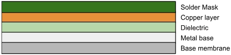
This structure consists of five distinct layers: a solder mask, copper trace layer (1 to 2 oz), thermally conductive dielectric (100 to 200 μm), metal base (usually aluminum), and an optional insulating back membrane.
It offers a direct thermal path from the component side through the dielectric to the metal base, enabling rapid heat transfer. With no plated through-holes, it’s optimal for metal core PCB LED arrays, drivers, and low-complexity power circuits where components are mounted on a single side.
If you’re working on projects that include Passive Infrared (PIR) Sensors, MCPCBs offer excellent thermal performance and are an ideal choice.
| Project Items | Our PCB Capabilities |
| Main Material Suppliers | Shengyi, Quanbao, Xintianyuan, Juding, etc. |
| Metal Types | Copper, Aluminum, Copper-Aluminum Composite, Stainless Steel, Iron |
| Structure | Single-layer, Double-layer/Multilayer, Copper/Aluminum Core, Thermal-Electric Separation |
| Thermal-Electric Separation Flatness | No significant difference(copper core boards) |
| Copper/Aluminum Core Thickness | 0.4–3.2 mm |
| Copper Thickness | (0.33, 0.5, 1, 2, 3, 4, 5, 6) oz, 6–10 oz requires confirmation |
| Insulation Layer Thickness | Thermal conductive insulation: 50, 75, 100, 125, 150 μm Others: FR4 bonding sheets |
| Thermal Conductivity | Standard FR4, 1 W/m·K, 2 W/m·K, 3 W/m·K, up to 15 W/m·K |
| Max Finshed Board Size – excl. Cu Core & Thermal-Electric Separation | 22.5″ × 30″ |
| PTH | Copper Base Thickness <0.8 mm: 0.8–6.0 mm Copper Base Thickness 0.8–1.6 mm: 1.0–8.0 mm Copper Base Thickness 1.7–3.2 mm: 1.2–8.0 mm |
| Countersink Holes | Vertical angle: 90° ± 5° Min drill bit: 0.8 ± 0.15 mm, Can be enlarged if needed Depth tolerance: ±0.20 mm |
| Counterbore Holes | Min angle: 30° ± 5°, Max angle: 180° Min drill bit: 0.8 ± 0.15 mm, Max drill bit: 6.0 ± 0.15 mm Depth tolerance: ±0.20 mm |
