How to Route PCB Traces: A Beginner Guide to Routing & Width
Let's explore PCB trace width, signal integrity and effective component placement, ensuring the connections of your board design are robust and efficient.
Get Your PCB Quote!

Table of Contents
Table of Contents
Ever wondered how the intricate electronic components on a circuit board manage to communicate with each other, transmitting signals and power seamlessly? The unsung heroes behind this marvel are PCB traces. If you’re new to designing printed circuit boards (PCBs) and find the concept of trace routing a bit daunting, you’re in the right place. This comprehensive guide will demystify PCB traces, breaking down complex ideas into simple, practical tips tailored for beginners.
From understanding what a trace is to mastering essential routing techniques, we’ll equip you with the knowledge needed to create functional and reliable designs for your first PCB project. We’ll explore crucial aspects like trace width, signal integrity, and effective component placement, ensuring your connections are robust and efficient. Whether you’re a hobbyist or an aspiring engineer, prepare to dive into the foundational technology that powers all modern electronics.
1. What is a PCB Trace?
At its core, a PCB trace is a thin, conductive pathway etched onto a printed circuit board. Imagine tiny highways on your circuit board, allowing electrical signals and power to travel between various electronic components, such as resistors, capacitors, and integrated circuits. These traces are typically made of copper, a highly conductive material, and are meticulously designed to ensure reliable electrical connections.
The layout and routing of these copper pathways are paramount to the performance and reliability of any electronic circuit. Without properly designed PCB traces, even the most advanced components cannot function as intended. They are the arteries and veins of your electronic device, carrying the lifeblood of electricity and data. Understanding the fundamental role of a PCB trace is the first step towards successful PCB design.
2. Why PCB Trace Design Matters
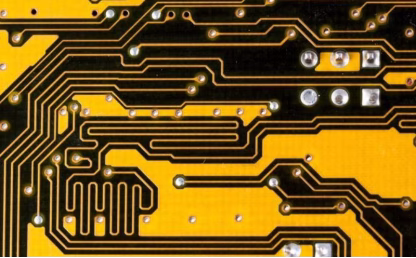
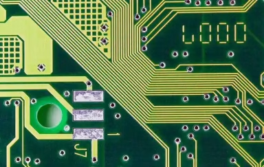
(yellow PCB routing)
The significance of meticulous PCB trace design extends far beyond simply connecting components. The way traces are routed, their dimensions, and their proximity to other elements profoundly impact the circuit’s overall performance. Poor trace design can lead to a host of problems, compromising the functionality and reliability of your electronic device. Here are the key areas where trace design plays a critical role:
2.1 Signal Integrity
Signal integrity refers to the quality of an electrical signal as it travels along a trace. A well-designed trace ensures that signals arrive at their destination without distortion, reflections, or excessive noise. Factors like trace length, impedance matching, and routing patterns directly influence signal integrity. In high-speed applications, maintaining excellent signal integrity is crucial to prevent data errors and ensure accurate operation.
2.2 Current Capacity
Every trace must be capable of carrying the electrical current required by the components it connects without overheating or experiencing significant voltage drops. The current capacity of a trace is primarily determined by its width and thickness. Traces that are too narrow for the current they carry can become hot, potentially damaging the PCB or leading to premature component failure. This is why a proper understanding of trace width calculation is essential, often guided by IPC standards and online calculators.
2.3 Electromagnetic Interference (EMI)
Electromagnetic interference (EMI ) occurs when electromagnetic fields generated by one part of a circuit interfere with another, leading to unwanted noise or malfunctions. PCB traces can act as antennas, both emitting and receiving EMI. Proper routing techniques, such as keeping traces short, maintaining appropriate trace spacing, and incorporating a robust ground plane, are vital for minimizing EMI and ensuring the circuit operates cleanly.
2.4 Manufacturability and Cost
Beyond electrical performance, trace design also impacts the ease and cost of manufacturing. Designs with unnecessarily complex routing, extremely narrow traces, or tight spacing can increase production costs and potentially lead to manufacturing defects. Adhering to manufacturer guidelines and designing for manufacturability (DFM) ensures a smoother and more cost-effective production process.
Need PCB Manufacturing or Assembly?
Get a free quote within 24 hours. We specialize in prototype-to-production PCB/PCBA for hardware teams worldwide.
3. Key PCB Trace Design Parameters
To create effective and reliable PCBs, designers must pay close attention to several critical parameters of their traces. These parameters dictate how signals behave and how much current a trace can safely handle.
3.1 Trace Width
Trace width is arguably one of the most crucial and challenging aspects of PCB design. It directly affects a trace’s current capacity and resistance. Wider traces have lower resistance, dissipate less heat, and can carry more current. Conversely, narrower traces are suitable for low-current signal lines but are more susceptible to resistance and heat buildup if over-currented. Experienced designers often use a PCB trace current calculator, or formulas based on IPC standards, to determine the appropriate width for a given current load and temperature rise.
For beginners, a good rule of thumb is to use wider traces for power and ground connections (e.g., 0.5mm or wider), and narrower traces for signal lines, while always considering the current requirements. A common industry standard (IPC-2152) provides detailed guidelines for various trace widths and current capacities under different conditions.
| Trace Type | Typical Width (Approximation) | Primary Concern |
| High Current (Power/Ground) | 0.5mm – 2.5mm+ | Current capacity, heat dissipation |
| General Signal | 0.15mm – 0.25mm | Signal integrity, manufacturability |
| High-Speed Signal | 0.1mm – 0.15mm | Controlled impedance, signal integrity |
3.2 Trace Length
The length of a trace significantly impacts signal integrity, especially in high-frequency applications. Longer traces can act like antennas, picking up or emitting EMI, and are more prone to signal degradation, reflections, and propagation delays. For critical high-speed signals, it’s best to keep traces as short and direct as possible. When length matching is required for differential pairs , ensure traces are routed in parallel and of equal length to maintain signal integrity.
3.3 Trace Spacing
Trace spacing refers to the distance between adjacent traces. Proper spacing is vital to prevent electrical shorts, crosstalk (where signals interfere with neighboring traces), and to ensure sufficient isolation between high-voltage lines. The minimum spacing is often dictated by manufacturing capabilities and design rules, but wider spacing generally improves signal isolation and reduces the risk of EMI. It’s also crucial for preventing arcing between high-voltage traces.
3.4 Trace Angles
When routing traces, avoid sharp 90-degree bends. These abrupt angles can create impedance discontinuities, causing signal reflections and increasing EMI. Instead, use 45-degree angles or smooth arcs when changing trace direction. This practice improves signal integrity and contributes to better overall circuit performance. Most modern PCB design software will offer options for 45-degree routing by default.

4. Essential PCB Routing Techniques for Beginners
Successfully routing your first PCB project involves a blend of strategic planning and adherence to best practices. Here are some fundamental techniques to get you started:
4.1 Plan Component Placement First
Before you even begin routing traces, the most crucial step is thoughtful component placement. Group related components together (e.g., power supply section, microcontroller, connectors). Position connectors and user interfaces at the board’s edges. Place decoupling capacitors close to the power pins of ICs. A well-organized component layout naturally leads to shorter, cleaner traces and simplifies the routing process immensely.
4.2 Prioritize Power and Ground Traces
Start your trace routing with the most critical connections: power and ground. These traces often carry higher currents and are fundamental to the stability of your circuit. Make power traces adequately wide to handle the current (refer back to trace width guidelines). For ground connections, consider using a solid ground plane (a large copper pour connected to ground) if your board has multiple layers. A robust ground plane significantly improves signal integrity and reduces EMI.
4.3 Manual Routing for Critical Connections
While auto-routers can be tempting, especially for beginners, it’s highly recommended to perform manual routing for critical connections. This includes high-speed signals, differential pairs, analog signals, and power lines. Manual routing gives you precise control over trace length, spacing, and impedance, allowing you to optimize performance and troubleshoot potential issues more effectively. Tools like KiCad and Eagle offer excellent manual routing features that guide you through the process.
4.4 Utilize Autorouting for Simpler Connections
For less critical, non-high-speed signal connections, autorouting can be a time-saver. After you’ve manually routed your critical paths, you can let the autorouter handle the remaining connections. However, always review the autorouter’s work. Autorouted traces can sometimes be meandering or create unnecessary vias, which might impact performance or manufacturability. Adjust them manually if needed to optimize trace length and clarity.
4.5 Set and Follow Design Rules (DRC)
Before any routing begins, set up your design rules (DRC) in your PCB layout software. These rules define minimum trace width, trace spacing, via sizes, and other manufacturing constraints. Adhering to these rules ensures your board is manufacturable and prevents common design errors. Regularly run the DRC check throughout your routing process to catch violations early.
5. Tools and Tips for Your First PCB Project
Embarking on your first PCB design journey can be exciting. Here are some practical tools and tips to ensure a smooth experience:
5.1 Embrace Beginner-Friendly PCB Design Software
For beginners, free and open-source tools like KiCad and Eagle (with a free tier) are excellent starting points. They offer comprehensive features, extensive component libraries, and a large community for support. These tools guide you through the entire PCB design workflow, from schematic capture to layout and Gerber file generation.
5.2 Understand the PCB Design Workflow
A typical PCB design workflow involves several distinct stages:
1) Schematic Creation: Design your circuit diagram.
2) Footprint Assignment: Link physical component shapes (footprints) to your schematic symbols.
3) Component Placement: Arrange components on the board.
4) Trace Routing: Connect components with traces.
5) Design Rule Check (DRC): Verify your design against manufacturing rules.
6) Export Gerbers: Generate manufacturing files for your board house.
7) Order Boards: Send your Gerber files to a PCB manufacturer.
Following this structured approach, as outlined by Schemalyzer, makes the process manageable and reduces errors.
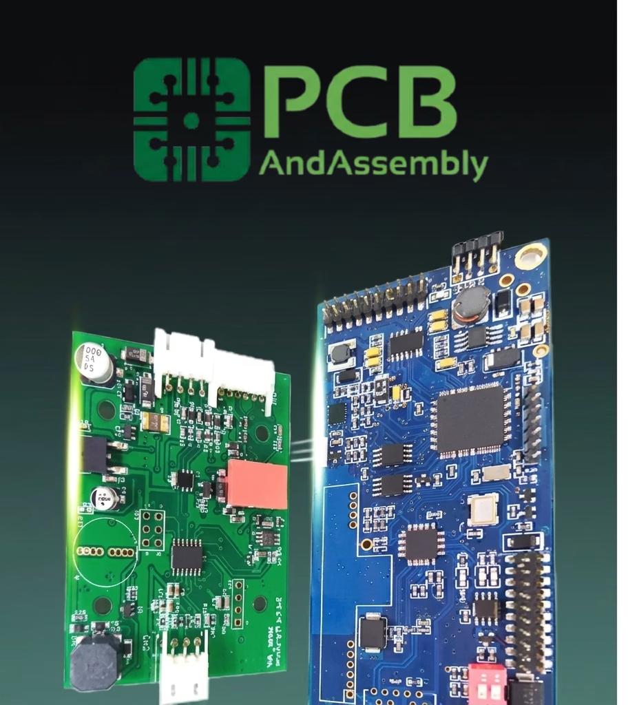
About PCBAndAssembly
Time is money in your projects – and PCBAndAssembly gets it. PCBAndAssembly is a PCB assembly company that delivers fast, flawless results every time. Our comprehensive PCB assembly services include expert engineering support at every step, ensuring top quality in every board. As a leading PCB assembly manufacturer, we provide a one-stop solution that streamlines your supply chain. Partner with our advanced PCB prototype factory for quick turnarounds and superior results you can trust.
5.3 Start Simple with 2-Layer Boards
For your initial projects, stick to 2-layer PCBs. They are simpler to route and generally more forgiving for beginners. Once you’re comfortable with 2-layer designs, you can gradually move to more complex multi-layer boards that offer greater flexibility for routing high-density or high-speed circuits .
5.4 Always Include a Ground Plane
Even on a 2-layer board, dedicating one side (or a significant portion of it) to a solid ground plane is a best practice. This provides a low-impedance path for return currents, improves EMI suppression, and helps stabilize power delivery. If using a single layer for ground, strategically use vias to connect ground points on the component side to the ground plane on the opposite side.
5.5 Verify Footprints and Dimensions
Before sending your design for manufacturing, always double-check that the footprints in your layout perfectly match your actual components. A misaligned or incorrect footprint can render your PCB unusable. Print out your PCB layout at 1:1 scale and place your physical components on top to verify fit and alignment.
5.6 Don’t Be Afraid to Iterate
PCB design is an iterative process. Your first design might not be perfect, and that’s okay. Learn from mistakes, experiment with different routing strategies, and continuously refine your skills. The more you practice, the better you’ll become at anticipating potential issues and optimizing your designs.
6. PCB Trace FAQs
There’s no single “ideal” trace width; it depends on the current it needs to carry, the maximum allowable temperature rise, and the board’s copper thickness. For signal traces, thinner widths are common (e.g., 0.15-0.25mm), while power traces require wider dimensions (e.g., 0.5mm+). Always consult a PCB trace current calculator or IPC standards based on your specific application.
Sharp 90-degree trace angles can cause impedance discontinuities, leading to signal reflections and increased electromagnetic interference (EMI), especially at high frequencies. They can also create acid traps during manufacturing. It’s best practice to use 45-degree angles or smooth arcs to ensure better signal integrity and manufacturability.
A ground plane is a large area of copper on a PCB layer that is connected to the circuit’s ground reference. It provides a low-impedance return path for currents, helps shield against EMI, and improves the overall stability of the power and signal distribution throughout the board. It’s crucial for maintaining signal integrity and reducing noise.
7. Summary
PCB traces are the lifeblood of any electronic device, serving as the conductive pathways that enable components to communicate and receive power. Mastering their design and routing is a foundational skill for anyone venturing into electronics. We’ve explored how critical parameters like trace width, length, and spacing directly impact signal integrity, current capacity, and the prevention of EMI.
By following a structured workflow, prioritizing thoughtful component placement, and understanding when to use manual versus autorouting techniques, beginners can confidently tackle their first projects. Tools like KiCad and Eagle, coupled with a commitment to setting and following design rules and incorporating a robust ground plane, will pave the way for successful and reliable PCB designs. Remember, practice and iterative refinement are key to becoming proficient in this essential aspect of electronics engineering.
Key Takeaways
- PCB traces are crucial copper pathways connecting components, influencing electrical performance and reliability.
- Proper trace width is vital for current capacity and preventing overheating; use calculators or IPC standards.
- Good trace routing minimizes EMI and ensures signal integrity, especially for high-speed signals.
- Always prioritize component placement before routing to optimize trace paths and shorten lengths.
- Avoid 90-degree trace bends; use 45-degree angles for better signal behavior and manufacturability.
- Implement a solid ground plane to enhance signal integrity and reduce noise.
- Utilize design rules (DRC) and tools like KiCad or Eagle for efficient and error-free design.

Get Quote Free