What is PCB Dielectric Material and How to Choose It?
The selection of PCB dielectric materials is a pivotal decision in modern electronics design, largely impacting performance, reliability and cost of the device.
Get Your PCB Quote!

Table of Contents
In the intricate world of Printed Circuit Boards (PCBs), every component plays a pivotal role in determining the final product’s performance, reliability, and longevity. Among these, the dielectric material — the non-conductive substrate that insulates the conductive layers — stands out as a critical element. Far from being a mere filler, the dielectric material profoundly influences a PCB’s electrical, thermal, and chemical properties, especially in demanding applications like high-speed data devices, 5G networks, and aerospace systems.
Choosing the right PCB dielectric material is a crucial step for designers, as it directly impacts signal integrity, power efficiency, and overall board reliability. A suboptimal choice can lead to signal loss, thermal issues, and even catastrophic failures, compromising the product’s functionality and lifespan. This comprehensive guide will walk you through the essentials of PCB dielectric material selection, breaking down key properties, common material types, and actionable insights to help you make an informed decision for your high-performance designs.
1. What is a PCB Dielectric Material?
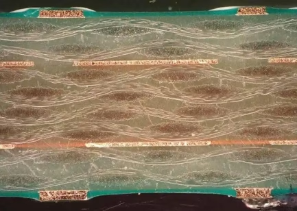
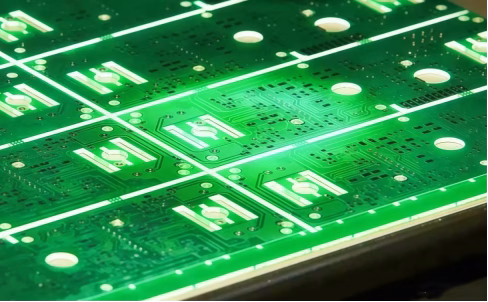
(Microscopic view of PCB substrate weave)
At its core, a PCB dielectric material is an electrical insulator that separates the conductive layers (typically copper traces) within a printed circuit board. Its primary function is to prevent electrical current from flowing between these layers while allowing electromagnetic fields to pass through. This non-conductive layer is fundamental to the structural and electrical integrity of a PCB.
The significance of the dielectric material becomes amplified in modern electronics, particularly in high-frequency PCB and high-speed designs. Here, the material’s ability to store and release electrical energy, its resistance to breakdown under voltage, and its stability across varying temperatures and environmental conditions are paramount. Without a carefully selected dielectric, even the most meticulously designed circuits would suffer from signal degradation, impedance mismatches, and reliability issues.
2. Key Properties of PCB Dielectric Materials
(green dielectric material layers)
To choose the best PCB dielectric material, you need to evaluate several critical properties. These characteristics dictate how the material will perform under specific electrical, thermal, and mechanical stresses:
1) Dielectric Constant (Dk)
The dielectric constant, often referred to as Dk, measures a material’s ability to store electrical energy in an electric field. It’s a dimensionless quantity that compares the capacitance of a material to that of a vacuum. A higher Dk means the material can store more energy. For high-speed designs, a stable and consistent Dk is essential to maintain signal integrity and controlled impedance. Variations in Dk, particularly within inhomogeneous anisotropic dielectrics like fiber/resin composites, can lead to differing effective dielectric constants depending on the trace location over fiber bundles or resin-rich areas.
2) Dissipation Factor (Df)
The dissipation factor, also known as dielectric loss or loss tangent, quantifies the amount of electrical energy lost as heat within the dielectric material when an alternating electric field is applied. A lower Df indicates less signal attenuation and better energy efficiency, which is critical for high-frequency and high-speed PCB applications (typically>1GHz). High Df materials can cause significant signal degradation and heat buildup, especially at higher frequencies.
3) Thermal Properties
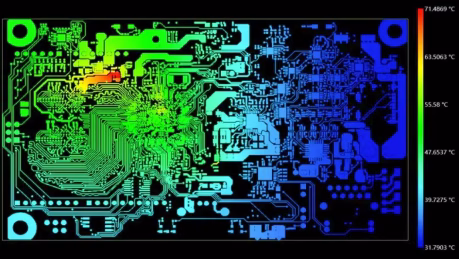
(PCB thermal simulation map)
Glass Transition Temperature (Tg): Tg is the temperature at which the dielectric material transitions from a rigid, glassy state to a softer, rubbery state. While the material doesn’t melt, its mechanical and electrical properties can change significantly above Tg. A higher Tg is desirable for applications subjected to high operating temperatures, ensuring dimensional stability during manufacturing processes like soldering and preventing warpage.
Decomposition Temperature (Td): Td is the temperature at which the material undergoes chemical decomposition, losing at least 5% of its mass. This temperature is a crucial indicator of a material’s thermal endurance and its ability to withstand extreme processing temperatures without degrading. A higher Td ensures the material remains stable during fabrication and operation.
Coefficient of Thermal Expansion (CTE): CTE measures how much a material expands or contracts with changes in temperature. A lower CTE, especially in the Z-axis (thickness), is preferable to minimize stress on plated through-holes (PTHs) and maintain structural integrity during thermal cycling. Mismatches in CTE between the dielectric and copper can lead to reliability issues.
Thermal Conductivity (k): This property indicates a material’s ability to conduct heat. Higher thermal conductivity is beneficial for applications requiring efficient heat dissipation, helping to manage the temperature of active components and prevent hotspots.
4) Dielectric Strength
Dielectric strength is the maximum electric field that a dielectric material can withstand without undergoing electrical breakdown. Measured in volts per mil (V/mil) or kilovolts per millimeter (kV/mm), it’s a measure of the material’s insulating capability. A high dielectric strength is critical for high-voltage applications to prevent arcing and short circuits between layers.
5) Moisture Absorption
This property indicates how much moisture a material absorbs from its environment. High moisture absorption can negatively impact Dk and Df, leading to performance degradation, especially in humid conditions. Low moisture absorption is desirable for maintaining stable electrical properties.
Understanding these properties is fundamental to selecting a PCB dielectric material that meets the specific requirements of your design, ensuring optimal electrical performance and reliability.
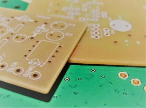
3. Common PCB Dielectric Materials
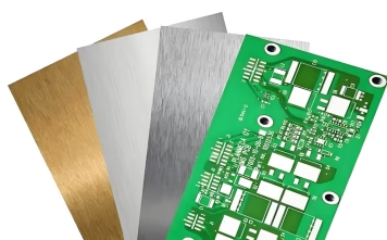
(common PCB dielectric material types)
A wide array of dielectric materials is available, each with unique characteristics suited for different applications. Here are some of the most common types:
1) FR-4 (Flame Retardant 4)
FR-4 is the most widely used PCB substrate material due to its excellent balance of electrical, mechanical, and thermal properties, coupled with its cost-effectiveness. It’s a composite material made of woven fiberglass cloth with an epoxy resin binder. While suitable for general-purpose electronics, its Dk and Df can be too high for very high-frequency applications, leading to signal loss. Modern variations of FR-4 with improved Dk/Df are available for slightly higher performance requirements.
2) PTFE (Polytetrafluoroethylene)/Teflon
Often known by its brand name Teflon, PTFE is a fluoropolymer characterized by its exceptionally low dielectric constant (Dk ≈ 2.0-2.2) and very low dissipation factor (Df < 0.001). These properties make PTFE an ideal choice for high-frequency PCB and RF/microwave applications where signal integrity and minimal loss are paramount. PTFE materials also exhibit excellent thermal stability, chemical resistance, and moisture resistance. However, they are typically more expensive and can be more challenging to process than FR-4.
3) Polyimide
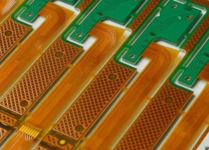
(Polyimide flexible PCB substrate)
Polyimide materials offer superior thermal stability, chemical resistance, and mechanical strength compared to FR-4. They are often used in high-temperature environments, flexible PCBs, and rigid-flex designs due to their flexibility and ability to withstand extreme conditions. While their electrical performance is better than standard FR-4, it’s generally not as good as PTFE for extremely high-frequency applications.
4) High Dk PCB Materials
Specialized high dielectric PCB materials are engineered for specific high-frequency circuit applications, typically above 1 GHz. These materials are characterized by a high dielectric constant (Dk > 10) and low dielectric loss (Df < 0.01). The primary benefit of high Dk materials is their ability to enable more compact signal transmission structures, allowing for miniaturization and integration in densely packed circuits. They are often used in applications like antenna substrates, power amplifiers, and RF modules. Examples include certain ceramic-filled hydrocarbon thermosets or specialized ceramic-based composites.
5) Other Specialized Materials
Hydrocarbon Ceramics: These offer a balance of excellent high-frequency performance (low Df, stable Dk) and improved thermal management compared to PTFE. They are often used in high-power RF applications.
Ceramic-Filled PTFE Composites: Combine the low loss of PTFE with improved dimensional stability and thermal conductivity due to ceramic fillers.
Modified Epoxies: These are enhanced versions of FR-4, offering improved thermal performance (higher Tg), lower Dk/Df, or better moisture resistance for intermediate performance requirements.
Here’s a comparison of some common dielectric materials:
| Material Type | Typical Dk (1GHz) | Typical Df (1GHz) | Typical Tg (°C) | Key Applications |
| FR-4 (Standard) | 4.2 – 4.7 | 0.018 – 0.025 | 130 – 180 | General purpose, low-frequency, digital circuits |
| FR-4 (High Performance) | 3.8 – 4.1 | 0.010 – 0.015 | 170 – 2 20 | Mid-range digital, some RF/microwave |
| PTFE/Teflon | 2.0 – 2.2 | 0 .0009 – 0.0015 | >280 (Decomposition Temp) | RF/Microwave, millimeter-wave, high-frequency radar |
| Polyimide | 3.2 – 3.4 | 0.005 – 0.010 | 220 – 250 | Flexible PCBs, high-temp applications, harsh environments |
| High Dk Materials | > 10 | < 0.01 | Varies | Antennas, power amplifiers, compact RF modules |
4. How to Choose Your PCB Dielectric Material?
Selecting the optimal PCB dielectric material is a multifaceted decision that requires careful consideration of several interconnected factors related to your application’s requirements:
1) Application Requirements
The ultimate purpose of your PCB is the primary driver. Is it for a consumer electronics device, an aerospace system, a medical implant, or a high -speed data server? Each domain imposes specific demands on performance, reliability, and environmental resilience.
High-Frequency/High-Speed Designs: For signals operating above 1 GHz or with fast rise times, materials with low Dk and ultra-low Df (like PTFE or specialized hydrocarbon ceramics) are essential to minimize signal loss and maintain impedance control.
High-Voltage Applications: Prioritize materials with high dielectric strength to prevent breakdown and arcing.
Thermal Management: If your board generates significant heat or operates in high-temperature environments, consider materials with high Tg, Td, and potentially higher thermal conductivity to prevent delamination and ensure operational stability.
Mechanical Flexing: For flexible or rigid-flex PCBs, polyimide-based materials are the go-to choice due to their excellent mechanical flexibility and endurance.
2) Electrical Performance Considerations

Signal Integrity: Stable Dk across frequency and temperature is vital for consistent impedance and minimal signal distortion. Lower Df reduces insertion loss.
Impedance Control: The Dk of the material directly influences trace impedance. Precise Dk values are needed to achieve the target impedance for transmission lines.
Power Handling: For power delivery networks, the dielectric strength and thermal properties become more critical.
3) Thermal and Environmental Factors
Operating Temperature Range: Ensure the material’s Tg and Td are well above the maximum expected operating and processing temperatures.
Moisture and Chemical Resistance: Applications in harsh or humid environments require materials with low moisture absorption and good chemical resistance to prevent performance degradation and corrosion.
Reliability: Long-term stability under thermal cycling, vibration, and humidity is crucial for critical applications.
4) Manufacturing and Cost Implications
Fabrication Ease: Some materials, particularly advanced RF laminates, can be more challenging to drill, route, and process, potentially increasing manufacturing costs and lead times. FR-4 remains the easiest and most cost-effective to process.
Cost: High-performance materials like PTFE or specialized hydrocarbon ceramics are significantly more expensive than standard FR-4. Balance the performance requirements with the project budget. Sometimes, a high-performance FR-4 variant can offer a good compromise.
Availability: Ensure the chosen material is readily available from your preferred PCB manufacturer or supplier.
By thoroughly evaluating these factors, designers can confidently select a PCB dielectric material that ensures optimal performance, reliability, and manufacturability for their specific application.
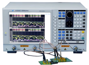
5. Testing Methods for Dielectric Materials
To ensure that chosen dielectric materials meet specifications and perform reliably, various testing methods are employed during material development and PCB manufacturing:
1) Dielectric Strength Testing
This test determines the maximum voltage a material can withstand before electrical breakdown occurs. The material sample is placed between two electrodes, and the voltage is gradually increased until a disruptive discharge (arcing) occurs. The dielectric strength is then calculated based on the breakdown voltage and the material’s thickness. This is crucial for high-voltage applications.
2) Dielectric Constant (Dk) and Dissipation Factor (Df) Measurement
Measuring Dk and Df accurately, especially at high frequencies, is complex. Common methods include:
Resonant Cavity Method: This method involves placing a dielectric sample inside a resonant cavity and observing changes in its resonant frequency and Q-factor. It’s highly accurate for specific frequencies.
Stripline Resonator Method: A stripline circuit is fabricated on the material sample, and its resonant frequencies are measured. This provides Dk and Df values across a range of frequencies relevant to actual PCB traces.
Split Post Dielectric Resonator (SPDR) Method: This is a non-destructive method often used for characterizing laminates at microwave frequencies.
3) Thermal Property Testing
Differential Scanning Calorimetry (DSC): Used to determine Tg by measuring the heat flow into or out of a sample as a function of temperature.
Thermogravimetric Analysis (TGA): Used to determine Td by measuring the mass loss of a material as it is heated.
Thermomechanical Analysis (TMA): Measures dimensional changes (like CTE) of a material as a function of temperature.
These tests are vital for validating material specifications and ensuring consistent performance across batches.
6. Expert Tips for Dielectric Material Selection
Navigating the vast landscape of PCB dielectric materials can be challenging. Here are some expert tips to guide your selection process:
Consult with Your Manufacturer Early: Engage your PCB manufacturer (like PCBAndAssembly) during the concept stage. Their engineering teams have extensive experience with various materials and can offer invaluable insights into manufacturability, cost implications, and lead times for specific materials.
Don’t Over-Specify(or Under-Specify): While it’s tempting to opt for the highest-performance material, it comes with a higher cost and potentially more complex manufacturing. Conversely, under-specifying can lead to performance issues. Strive for the best balance of performance, cost, and manufacturability for your specific application.
Consider the Entire Stack-up: The dielectric material doesn’t operate in isolation. Its properties interact with copper foil type, prepreg, and overall stack-up design. A holistic view is crucial for impedance control and signal integrity.
Understand Dk Variation: Be aware that Dk can vary with frequency, temperature, and even moisture content. For critical high-frequency applications, choose materials with stable Dk across the expected operating range. Remember that fiber/resin composites are inhomogeneous, leading to slight Dk variations depending on trace location.
Thermal Reliability is Key: Even if your design isn’t explicitly high-power, robust thermal properties (high Tg, Td, low Z-axis CTE) are crucial for long-term reliability during soldering, rework, and operational thermal cycling.
Prototype and Test: Whenever possible, prototype your design with the chosen material and perform thorough electrical and thermal testing under realistic operating conditions. This empirical validation is often the most reliable way to confirm material suitability.
7. PCB Dielectric Material FAQs
Dk (dielectric constant) measures a material’s ability to store electrical energy, impacting signal propagation speed and impedance. Df (dissipation factor) measures the energy lost as heat within the material, directly affecting signal attenuation and integrity, especially at high frequencies.
Standard FR-4 has a relatively higher Dk and Df compared to specialized high-frequency materials. At higher frequencies, its Dk causes signals to propagate slower and its higher Df leads to significant signal loss, making it unsuitable for applications requiring minimal attenuation and precise impedance control.
A “high dielectric” PCB material is characterized by a significantly high dielectric constant (typically Dk > 10) and low dielectric loss (Df < 0.01). These materials are specialized for high-frequency circuits where miniaturization and compact signal structures are desired, such as in antennas or RF power amplifiers.
8. Summary
The selection of PCB dielectric materials is a pivotal decision in modern electronics design, profoundly impacting performance, reliability, and cost. From the ubiquitous FR-4 to specialized PTFE and high Dk materials, each substrate offers a unique blend of electrical, thermal, and mechanical properties. Understanding key characteristics such as dielectric constant (Dk), dissipation factor (Df), thermal stability (Tg, Td), and dielectric strength is paramount for making an informed choice. For high-speed and high-frequency applications, prioritizing materials with low Dk and ultra-low Df is critical to maintain signal integrity and minimize losses. Collaborating with experienced PCB manufacturers and rigorously testing prototypes are essential steps to ensure the chosen material meets the stringent demands of your specific application, paving the way for reliable and high-performing electronic products.

Get Quote Free