3-Layer PCBs: Why You Rarely See Them
3-layer PCBs are uncommon due to poor cost-effectiveness compared to 2-layer and 4-layer alternatives. A 3-layer PCB typically uses a Signal-Ground-Signal (S-G-S) or Signal-Power-Signal (S-P-S) configuration, with the internal layer providing a reference plane .se from 2 to 3 layers is significant, while the performance gain is modest.
Get Your PCB Quote!

1. Introduction
In the vast landscape of electronics, printed circuit boards (PCBs) are the unseen highways carrying electrical signals that power everything from your smartphone to advanced industrial machinery. While 2-layer PCBs dominate simple designs and 4, 6, 8, or even higher layer counts are standard for complex, high-performance applications, there’s a peculiar absence in the middle: the 3-layer PCB. Despite the logical progression, this specific configuration remains a rare sight in mass production. Why is this so? What unique challenges or advantages does it present that lead to its infrequent adoption? This deep dive will unravel the mystery of the 3-layer PCB, exploring its theoretical structure , the practical reasons for its scarcity, and the highly specific scenarios where it might – just might – find its purpose.
2. Unpacking the Theoretical 3-Layer PCB Stackup
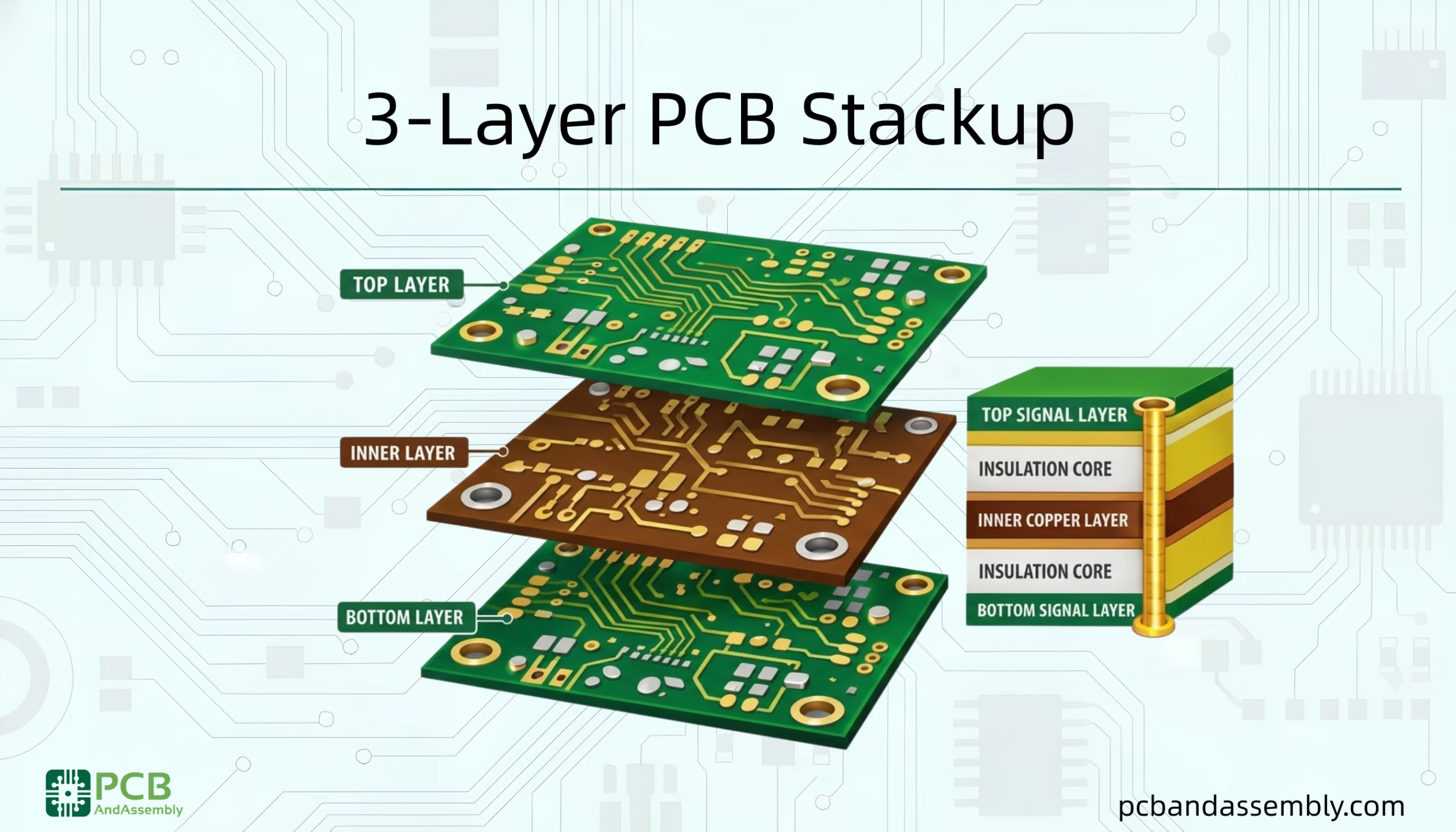
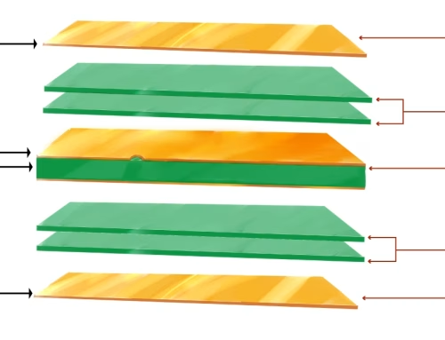
To understand why 3-layer PCBs are rare, we first need to visualize their construction. A multi-layer PCB is built by laminating multiple layers of copper traces separated by insulating dielectric material. For a 3-layer board , there are primarily two common theoretical stackup configurations:
- Signal – Ground – Signal (S-G-S):In this configuration, the top and bottom layers are used for routing signal traces, while the middle layer is a dedicated ground plane. The ground plane serves as a consistent reference for the signals on the outer layers, which is crucial for controlling impedance and reducing noise.
- Signal – Power – Signal (S-P- S):Less common but theoretically possible, this setup would place a power plane in the middle. While a power plane can also act as a reference, a dedicated ground plane is generally preferred for its superior EMI shielding capabilities and stable reference for high -frequency signals.
The key takeaway here is the inclusion of an internal plane. This single internal plane is the defining characteristic that separates a 3-layer board from a simpler 2-layer design, aiming to offer improved electrical performance.
3. Why 3-Layer PCBs Are Rarely Used
The primary reason for the rarity of 3- layer PCBs boils down to an unfavorable cost-to-benefit ratio when compared to their 2-layer and 4-layer counterparts. The slight advantages offered by a third layer are often outweighed by the increased cost and manufacturing complexity, especially when a 4-layer board offers significantly more for a marginally higher price.
3.1. The 2-Layer Advantage
For a vast majority of electronic devices, a 2-layer PCB is perfectly adequate. These boards consist of a top signal layer and a bottom signal layer, separated by a dielectric. They are:
- Cost-Effective:Significantly cheaper to manufacture due to fewer layers and simpler processing.
- Easier to Design:Layout is straightforward, and debugging is simpler.
- Sufficient for Low-Frequency/ Density Designs:For digital circuits running at moderate speeds or analog circuits with less stringent signal integrity requirements, 2-layer boards are the go-to.
Adding a third layer for a modest improvement in signal integrity or routing density often doesn’t justify the additional manufacturing cost for projects that could otherwise be done on two layers. The cost increase for that extra layer is substantial relative to the cost of a 2-layer board.
3.2. The 4-Layer PCBs
This is the crux of the issue. When a design outgrows a 2-layer board, the logical and most cost-effective next step is almost always a 4-layer PCB. A standard 4-layer stackup typically includes:
- Layer 1: Signal (Top)
- Layer 2: Ground Plane
- Layer 3: Power Plane
- Layer 4: Signal (Bottom)
The benefits of a 4-layer board are immense:
- Dedicated Ground and Power Planes:These provide excellent reference planes for signals, significantly improving signal integrity, controlling impedance, and reducing crosstalk. They also offer superior EMI (Electromagnetic Interference) shielding.
- Higher Routing Density:With two dedicated signal layers and two internal planes, designers have much more room to route complex circuits, making it suitable for dense component placement.
- Thermal Management:Internal planes can help dissipate heat more effectively.
Crucially, the manufacturing cost difference between a 3-layer and a 4-layer PCB is often negligible. The setup costs for processing multiple layers, preparing prepreg and core materials, and the lamination cycle are largely similar once you move beyond two layers. Therefore, designers and manufacturers usually opt for the “free” extra layer and its substantial benefits by going straight to 4 layers, rather than settling for the limited advantages of three.
3.3. Manufacturing Complexity and Yield
Each additional layer increases the complexity of the PCB manufacturing process. More layers mean:
- More drilling operations and precise alignment needed for vias (vertical interconnects).
- Additional lamination steps, which introduce opportunities for defects like voids or delamination.
- Tighter tolerances for etching and registration between layers.
While a 3-layer board is less complex than a 4-layer, the jump in complexity from 2 to 3 layers is significant. The marginal reduction in complexity from 4 to 3 layers often doesn’t translate into a meaningful cost saving or yield improvement that would make it more attractive than a full 4-layer stackup.
3.4. Limited Routing & Signal Integrity Benefits
While a 3-layer PCB with a central ground plane offers better signal integrity and EMI performance than a 2-layer board, its benefits are still limited compared to a 4-layer. With only two signal layers and one reference plane, designers often find themselves still struggling with routing congestion for complex designs. High-speed signals still need careful planning to ensure they always reference a consistent plane, and the lack of a dedicated power plane means power delivery networks might still suffer from higher impedance and noise.
4. When a 3-Layer PCB Might Make Sense
Despite the overwhelming arguments against it, there are a few highly specific, niche scenarios where a 3-layer PCB could theoretically offer a unique advantage. These are typically driven by very particular design constraints or cost sensitivities that make the standard 2-layer or 4-layer options less ideal.
4.1. Cost-Sensitive Designs with Specific Signal Integrity Needs
Imagine a project that is extremely cost-sensitive, making a 4-layer board prohibitive, yet requires better signal integrity than a 2-layer board can provide for a few critical traces. For instance, a simple mixed-signal board where a low-noise analog section desperately needs a clean ground reference, but the digital section is minimal . In such a hypothetical scenario, a 3-layer (S-G-S) could be considered if the cost savings over a 4-layer are demonstrably significant and the benefits gained are precisely what the design needs without demanding the full capabilities of a 4-layer. This is a very fine line to walk and requires careful cost-benefit analysis.
4.2. Unique Impedance Control Requirements
Occasionally, a design might have one or two extremely critical high-speed traces that require very precise impedance control. If these traces can be strategically placed on one of the outer layers and referenced to the single internal ground plane, while the rest of the board’ s signals are less critical, a 3-layer board might offer a targeted solution. This is, again, a highly specialized situation, as usually, if impedance control is a concern, multiple layers are required for numerous signals.
4.3. Educational and Experimental Purposes
In academic or research settings, a 3-layer PCB could serve as an excellent educational tool. It allows students or researchers to specifically study the impact of introducing a single internal reference plane on signal integrity, EMI, and routing density, without immediately jumping to the complexities of a full 4-layer board. It provides a transitional step in understanding multi-layer PCB design principles.
5. 2-Layer vs. 3-Layer vs. 4-Layer PCBs: A Comparative Look
To further illustrate why the 3-layer option is so rarely chosen, let’s compare its characteristics with the more common 2-layer and 4-layer configurations.
| Feature | 2-Layer PCB | 3-Layer PCB (S-G- S) | 4-Layer PCB (S-G-P-S) |
| Typical Stackup | Signal – Signal | Signal – Ground – Signal | Signal – Ground – Power – Signal |
| Relative Cost | Low (Baseline) | Medium (Significant increase over 2-layer) | Medium-High (Marginal increase over 3-layer) |
| Routing Density | Low (Limited space, crosstalk issues) | Medium-Low (Slightly better due to internal plane clearance) | High (Dedicated signal layers, internal planes) |
| Signal Integrity | Basic (Poor impedance control) | Improved (Better reference for outer layers) | Excellent (Dedicated ground & power planes for reference) |
| EMI Performance | Poor (No internal shielding) | Moderate (Internal ground plane offers some shielding) | Good (Solid ground and power planes provide excellent shielding) |
| Power Delivery | Difficult (Trace routing for power) | Challenging (No dedicated power plane) | Excellent (Dedicated power plane with low impedance) |
| Best Use Cases | Simple, low-frequency , non-critical designs | Very niche, cost-constrained designs needing minimal SI improvement over 2-layer | Complex, high-speed, mixed-signal designs, high-density components |
6. 3-Layer PCB FAQ
(1) What is the most common PCB layer count?
2-layer and 4-layer PCBs are by far the most common in commercial electronics. 2-layer boards are used for simpler, cost-effective designs, while 4-layer boards are the entry point for more complex, high-performance applications requiring better signal integrity and routing density.
(2) Does a 3-layer PCB offer better EMI shielding than a 2-layer?
Yes, a 3-layer PCB with an internal ground plane (S -G-S) typically offers better EMI shielding and signal integrity compared to a 2-layer PCB. The ground plane acts as a shield and provides a consistent return path for signals, which helps reduce electromagnetic emissions and susceptibility.
(3) Why is the jump from 2 to 4 layers often preferred over 2 to 3 layers?
The manufacturing cost difference between a 3-layer and a 4- layer PCB is often minimal. For this marginal additional cost, a 4-layer board provides significantly more benefits, including dedicated ground and power planes, superior signal integrity, vastly improved EMI performance, and much higher routing density, making it a far better return on investment for most designs that outgrow 2-layer capabilities.
7. Summary
The 3-layer PCB stands as an intriguing anomaly in the world of electronics manufacturing. While theoretically possible and offering some advantages over a 2-layer board, its practical application is severely limited. The primary hurdle is its unfavorable cost-to-benefit ratio; the leap from 2 to 3 layers incurs significant manufacturing costs without delivering proportional performance gains that a 4-layer board provides for a marginally higher price. For most designs, a 2-layer board suffices for simplicity and cost, or a 4-layer board becomes necessary for high -performance and complexity, rendering the 3-layer option largely obsolete outside of very specific, niche constraints or educational contexts.

Get Your PCB Quote!