4-Layer PCB: What is it & Stackup & Manufacturing
Learn what a 4-layer PCB is, how its stackup works, and what makes it the go-to choice for high-speed, high-density electronics design. PCBAndAssembly offers expert PCB manufacturing services that can help you create efficient and reliable 4-layer PCBs tailored to your project needs.
Get Your PCB Quote!
Table of Contents
- 1. Einleitung
- 2. Was ist eine 4-Layer-Leiterplatte?
- 3. 4-Layer PCB Materials and Specifications
- 4. 4-Schicht-Leiterplattenmaterialien
- 5 . Key Advantages of Using a 4-Layer PCB Stackup
- 6. Common 4-Layer PCB Stackup Configurations
- 7.ritical Design Considerations and Best Practices
- 8. 4-Layer PCB Manufacturing Process Highlights
- 9. 4-Layer PCB FAQ
- 10 Zusammenfassung

1. Introduction
In the intricate world of electronics, the Printed Circuit Board (PCB) serves as the backbone, connecting components and enabling device functionality. As modern devices become more compact, complex, and high-speed, the demands on PCB design intensify. While a simple two-layer PCB suffices for many applications, the rise of sophisticated embedded systems, IoT devices, and high-frequency communication necessitates advanced solutions. This is where the 4-layer PCB stackup comes into play, offering a critical balance of performance, size, and cost.
2. What is a 4-Layer PCB?
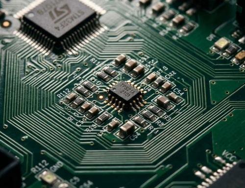
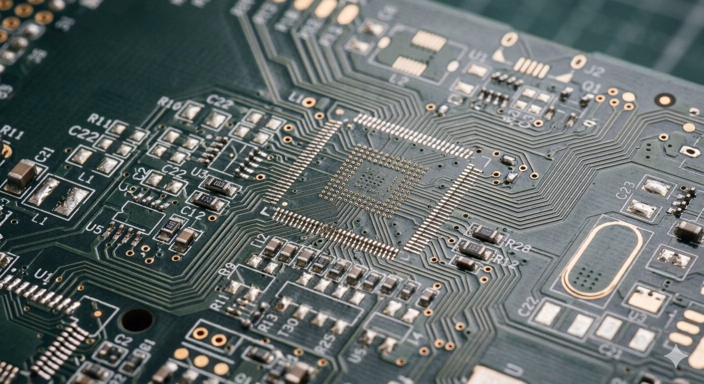
A 4-layer PCB is a type of multi-layer PCB composed of four conductive copper layers separated by insulating dielectric materials. Unlike a single or double-sided PCB, which routes all traces on external layers or two layers respectively, a 4-layer PCB incorporates internal layers for routing signals, providing dedicated ground planes, and power planes. This architecture offers significantly more flexibility and performance benefits.
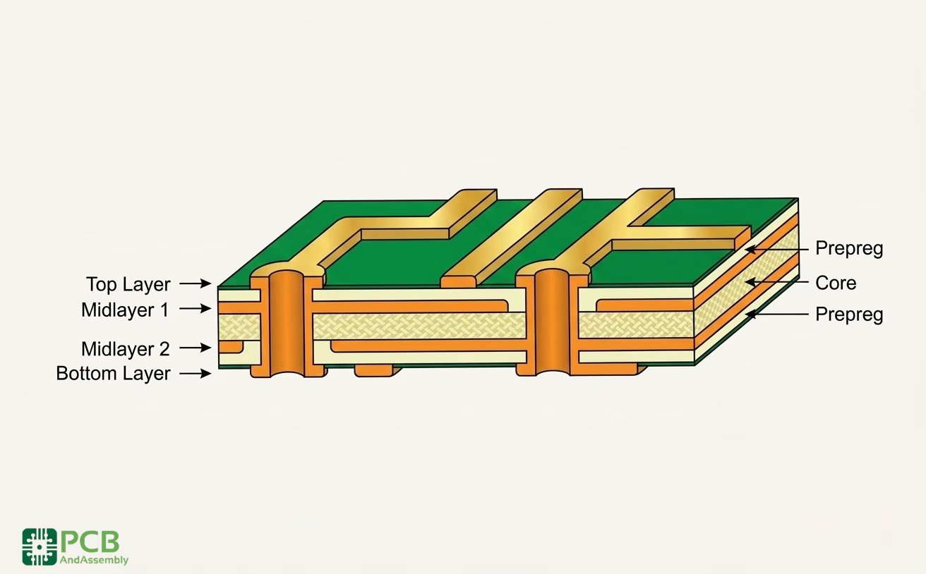
Typically, a 4-layer PCB is constructed by laminating together two outer layers (often referred to as top and bottom signal layers) with two inner layers (commonly used for ground and power planes) using prepreg and core materials under high temperature and pressure.
3. 4-Layer PCB Materials and Specifications
The materials used in 4-layer PCB manufacturing are crucial for its performance characteristics, especially its electrical properties and reliability. The most common material is FR-4, a glass-reinforced epoxy laminate known for its good electrical insulation, mechanical strength, and cost-effectiveness. Key material specifications include:
- Dielectric Constant (Dk or Er):A measure of how easily an electric field passes through the material. For FR-4, it’s typically around 4.2-4.7, varying with frequency.
- Loss Tangent (Df):Indicates the material’s energy loss. Lower Df is better for high-frequency applications.
- Glass Transition Temperature (Tg):The temperature at which the material transitions from a rigid to a rubbery state. Higher Tg materials are preferred for high -power applications.
The 4-layer PCB thickness is another important specification, typically ranging from 0.8mm (0.031 inches) to 1.6mm ( 0.063 inches), with 1.6mm being standard. The individual layer thicknesses (copper, prepreg, core) are precisely controlled to achieve desired impedance values.
Common Thickness Specifications and Use Cases
Designers typically select a board thickness based on the specific spatial constraints and structural requirements of the device:
- 8mm – 1.0mm: These thinner profiles are ideal for compact devices such as smartphones and portable electronics where space is at a premium.
- 2mm – 1.6mm: This is the most versatile range. The 1.6mm thickness is particularly cost-effective as fabricators optimize their processes around this standard.
- 0mm – 2.4mm: Increased thickness is utilized when the PCB requires higher rigidity to support heavy components, large connectors, or to withstand harsh environments.
Typical 1.6mm 4-Layer Stackup Breakdown
To achieve precise controlled impedance, manufacturers carefully manage the combination of copper foil, core material, and prepreg. A typical 1.6mm 4-layer PCB stackup is structured as follows:
| Component | Thickness (Typical) | Function |
| Top Copper | 35μm (1 oz) | Signal routing and component soldering |
| Prepreg (e.g., 1080) | 0.08mm | Insulates and bonds the top layer to the inner layer |
| Inner Layer 2 (Ground) | 35μm (1 oz) | Dedicated ground plane for signal return paths |
| Core (FR-4) | 1.2mm | Provides the primary structural support for the board |
| Inner Layer 3 (Power) | 35μm (1 oz) | Dedicated power plane for voltage distribution |
| Prepreg (e.g., 1080) | 0.08mm | Insulates and bonds the bottom layer to the inner layer |
| Bottom Copper | 35μm (1 oz) | Signal routing layer |
4. 4 Layer PCB Materials
Selecting the appropriate substrate and conductive materials is crucial for the reliability and electrical performance of a 4-layer PCB.
Base Material Properties (FR-4)
The most common material is FR-4, a glass-reinforced epoxy laminate known for its mechanical strength and cost-effectiveness. For high-speed designs, the following specifications are critical:
Dielectric Constant (Dk/Er): For FR-4, this typically ranges from 4.2 to 4.7. This value affects signal propagation speed and characteristic impedance.
Loss Tangent/Dissipation Factor (Df): This indicates the energy loss of the material; a lower Df is essential for maintaining signal integrity in high-frequency applications.
Glass Transition Temperature (Tg): This is the temperature at which the material transitions from rigid to a rubbery state.
- Standard Tg (130°C): Suitable for most cost-sensitive applications.
- High Tg (170-180°C): Required for lead-free assembly, automotive applications, or high-power systems.
Copper Weight Options
Copper weight (oz/ft²) determines the thickness of the conductive layers and their current-carrying capacity:
- 5 oz (17.5μm): Used for fine-pitch components and high-density, low-current signal routing.
- 0 oz (35μm): The standard choice for most signal and power applications in a typical 4-layer design.
- 0 oz – 3.0 oz (70μm – 105μm): Ideal for power electronics, motor drives, or high-current power supplies to manage heat and voltage drop.
Insulating Layers: Prepreg and Core
The 4-layer structure is built by laminating core (cured fiberglass) and prepreg (fiberglass pre-impregnated with resin).
- Prepreg:Acts as the “glue” that bonds the layers together under high temperature and pressure. Common styles like 1080 (0.08mm thin) or 7628 (0.2mm thick) are chosen based on the required insulation and layer spacing.
- Core: Provides the central foundation. The resin content in these materials affects how well they fill the gaps around the etched inner-layer copper features during the manufacturing process.
5 . Key Advantages of Using a 4-Layer PCB Stackup
Employing a 4-layer PCB stackup offers several compelling advantages over simpler designs, making it a preferred choice for many modern electronic systems:
- Improved Signal Integrity:Dedicated ground and power planes provide stable return paths for signals, reducing crosstalk and noise, and improving signal quality.
- Reduced Electromagnetic Interference (EMI):Well-designed power and ground planes act as natural shields, containing electromagnetic fields and minimizing radiation, leading to better EMC performance.
- Enhanced Power Delivery:A solid power plane ensures low impedance power distribution, critical for high-speed digital circuits that require stable voltage rails.
- Smaller Form Factor:The ability to route signals on internal layers allows for denser routing and more compact designs, enabling smaller product sizes.
- Better Thermal Management:Copper planes can assist in heat dissipation, though dedicated thermal management strategies are still often needed.
- Easier Impedance Control:With reference planes readily available, controlled impedance lines can be more precisely designed and manufactured, crucial for high -frequency signals.
6. Common 4-Layer PCB Stackup Configurations
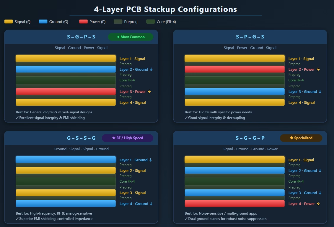
The arrangement of the four layers is critical. Each stackup configuration has its strengths and weaknesses, making it suitable for different applications. Here are the most common 4-layer PCB stackup configurations:
6.1. Signal-Ground-Power-Signal (S-G-P- S)
This is one of the most popular and recommended 4-layer PCB stackup configurations for general-purpose digital and mixed-signal designs.
- Layer 1 (Top):Signal Layer
- Layer 2:Ground Plane
- Layer 3:Power Plane
- Layer 4 (Bottom):Signal Layer
Advantages:
- Provides excellent shielding for the two outer signal layers, reducing EMI.
- Offers low impedance return paths for signals, enhancing signal integrity.
- Power and ground planes are adjacent, allowing for good decoupling capacitance between them, improving power delivery network (PDN) performance.
- Suitable for designs with both analog and digital signals, allowing segregation by routing sensitive analog signals on one outer layer and digital on the other.
Considerations: Managing routing density on the two outer layers is key.
6.2. Signal-Power-Ground-Signal (S-P-G- S)
This configuration also offers good performance but with a slightly different emphasis on plane arrangement.
- Layer 1 (Top):Signal Layer
- Layer 2:Power Plane
- Layer 3:Ground Plane
- Layer 4 (Bottom):Signal Layer
Advantages:
- Similar to S-G-P-S in providing dedicated power and ground planes.
- Maintains good signal integrity due to nearby reference planes.
- The close proximity of power and ground planes still offers good decoupling.
Considerations: The outer signal layers are not as tightly coupled to a single, large ground plane as in the S-G-P-S configuration, which might slightly impact EMI performance in some specific high-frequency scenarios.
6.3. Ground-Signal-Signal-Ground (G-S-S-G)
This stackup is particularly favored for high- frequency applications where critical signals need optimal shielding and impedance control.
- Layer 1 (Top):Ground Plane
- Layer 2:Signal Layer
- Layer 3:Signal Layer
- Layer 4 (Bottom):Ground Plane
Advantages:
- Provides excellent shielding for the internal signal layers, dramatically reducing EMI radiation.
- Each signal layer is adjacent to a solid ground plane, ensuring controlled impedance and superior signal integrity.
- Ideal for high-speed digital and RF designs where noise reduction and precise impedance matching are paramount.
Considerations: No dedicated power plane, meaning power routing might need to be done as traces on the signal layers or require careful stitching, which can complicate PDN design. This configuration is often chosen when power delivery is less critical or can be managed otherwise, and signal integrity is the absolute top priority.
6.4. Signal-Ground-Ground-Power (S-G-G-P)
This configuration is less common but can be useful in specific scenarios, especially those requiring multiple ground layers for noise suppression or thermal considerations.
- Layer 1 (Top):Signal Layer
- Layer 2 :Ground Plane
- Layer 3:Ground Plane (or split ground/power)
- Layer 4 (Bottom):Power Plane
Advantages:
- Offers two robust ground planes, which can be beneficial for reducing noise and managing heat.
- The top signal layer has an immediate ground reference.
Considerations: The two internal ground layers might be redundant for typical digital applications and could be better utilized for a power plane closer to the top signal layer. Routing on the bottom layer would reference the power plane, which is generally less ideal than a ground plane for signal return paths. This stackup is often adapted or customized rather than used in its strict form.
Here’s a quick comparison of the common 4-layer PCB stackup configurations:
| Configuration | Layer 1 (Top) | Layer 2 | Layer 3 | Layer 4 (Bottom) | Key Advantage | Primary Use Case |
| Signal-Ground-Power-Signal (S-G-P-S) | Signal | Ground | Power | Signal | Excellent Signal Integrity & EMI Reduction | General Digital, Mixed-Signal |
| Signal-Power-Ground-Signal (S-P-G-S) | Signal | Power | Ground | Signal | Good Signal Integrity & Decoupling | Digital with specific power needs |
| Ground-Signal- Signal-Ground (G-S-S-G) | Ground | Signal | Signal | Ground | Superior EMI Shielding & Controlled Impedance | High- Speed Digital, RF, Analog Sensitive Signals |
| Signal-Ground-Ground-Power (S-G-G-P) | Signal | Ground | Ground | Power | Robust Grounding, Specific Needs | Specialized applications requiring multiple grounds |
7. Critical Design Considerations and Best Practices
Beyond selecting the right stackup, several design practices are crucial to optimize performance and avoid common 4-layer PCB design mistakes:
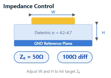
- Impedance Control:For high-speed signals, characteristic impedance must be controlled. This involves precise trace width, dielectric thickness, and dielectric constant relative to a reference plane. The S-G-P-S and G-S-S-G stackups are excellent for this.
- Power and Ground Plane Integrity:Ensure solid, unbroken power and ground planes. Avoid routing signal traces through these planes unless absolutely necessary, as this creates splits and degrades plane performance.
- Dec oupling Capacitors:Place decoupling capacitors close to IC power pins, connecting them between the power and ground planes to provide local current reservoirs and filter high-frequency noise.
- Via Stitching:Use stitching vias to connect ground planes on different layers, ensuring a low-impedance return path for signals and improving EMI performance.
- Trace Routing:Route high-speed signals adjacent to a solid ground plane. Keep traces short and avoid sharp 90-degree bends. Segregate sensitive analog signals from noisy digital signals whenever possible.
- Thermal Relief:When connecting pins to large copper planes, use thermal relief pads to prevent heat from rapidly dissipating during soldering , ensuring reliable solder joints.
- Layer Thickness and Material Selection:Work closely with your PCB manufacturer to select appropriate prepreg and core materials and thicknesses to achieve desired impedance values and overall 4-layer PCB thickness.
8. 4-Layer PCB Manufacturing Process Highlights
The 4-layer PCB manufacturing process involves several key steps that build upon simpler PCB fabrication:
Inner Layer Preparation: The two inner copper layers (typically ground and power) are etched with their respective patterns.
Lamination: These etched inner layers are then sandwiched between prepreg ( a fiberglass material pre-impregnated with epoxy resin) and a core layer, and then with outer copper foils. This entire stack is subjected to high temperature and pressure, causing the prepreg to flow and cure, bonding all layers together.
Drilling: After lamination, holes (vias) are drilled through the entire board.
Plating: The drilled holes are then plated with copper to create electrical connections between the layers.
Outer Layer Etching: The top and bottom (signal) layers are then etched to form the final trace patterns.
Solder Mask and Silkscreen: Solder mask is applied for insulation and protection, followed by silkscreen printing for component labels and markings.
Final Finish: A surface finish (e.g., HASL, ENIG) is applied to protect copper and ensure solderability.
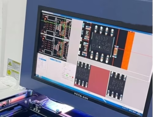
Testing: Electrical testing (e.g., bare board test) ensures connectivity and absence of shorts or opens.
9. 4-Layer PCB FAQ
Q1:When should I choose a 4-layer PCB over a 2-layer PCB?
A: A 4-layer PCB is recommended when your design involves high-speed signals, requires better EMI control, has dense component placement, or needs improved power delivery stability, which are common limitations of 2-layer boards.
Q2:What is the most common 4-layer PCB stackup?
A: The Signal-Ground -Power-Signal (S-G-P-S) stackup is widely considered the most common and versatile configuration for general-purpose digital and mixed-signal designs due to its balanced performance in signal integrity, EMI reduction, and power delivery.
Q3:How does a dedicated ground plane improve signal integrity?
A: A dedicated ground plane provides a continuous, low-impedance return path for high-frequency signals. This minimizes loop area, reduces inductance, and helps control characteristic impedance, all of which contribute to better signal quality and less noise.
Q4:What is the typical 4-layer PCB thickness?
A: The most common overall thickness for a 4-layer PCB is 1.6mm (0.063 inches), which is a widely adopted standard in the industry. However, thinner or thicker boards can be manufactured depending on specific application requirements .
Q5:Are there any disadvantages to using a 4-layer PCB?
A: The primary disadvantages are increased manufacturing cost compared to 2-layer PCBs, and a slightly longer manufacturing time. However, for complex or high-performance designs, these costs are often justified by the significant performance benefits.
10. Summary
The 4-layer PCB stackup is an indispensable tool in modern electronics design, bridging the gap between simple two-layer boards and highly complex multi-layer solutions. By carefully arranging signal, ground, and power layers, designers can achieve superior signal integrity, mitigate EMI, and ensure stable power delivery for increasingly sophisticated devices. Configurations like Signal-Ground-Power-Signal (S-G-P-S) and Ground-Signal-Signal-Ground (G-S-S-G) offer robust solutions for various applications, from general digital circuits to high-frequency RF systems.
Understanding the interplay between materials, stackup choices, and critical design practices is paramount to harnessing the full potential of these boards. Avoiding common design pitfalls and adhering to best practices ensures a reliable, high-performance product. As technology continues to push boundaries, the strategic application of 4-layer PCBs remains a foundational element for success.
Table of Contents
- 1. Einleitung
- 2. Was ist eine 4-Layer-Leiterplatte?
- 3. 4-Layer PCB Materials and Specifications
- 4. 4-Schicht-Leiterplattenmaterialien
- 5 . Key Advantages of Using a 4-Layer PCB Stackup
- 6. Common 4-Layer PCB Stackup Configurations
- 7.ritical Design Considerations and Best Practices
- 8. 4-Layer PCB Manufacturing Process Highlights
- 9. 4-Layer PCB FAQ
- 10 Zusammenfassung

Get Your PCB Quote!