Automated Optical Inspection Test in PCB
AOI technology is a step in modern PCB assembly, crucial for ensuring product quality, improving production efficiency, and enabling intelligent manufacturing.
Get Your PCB Quote!
Table of Contents
- 1Què és la inspecció òptica automatitzada (AOI)?
- 2.Per què són populars les proves AOI?
- 3.Com funciona l'AOI
- 4Defectes comuns detectats per AOI
- 5.Els avantatges de la prova AOI
- 6. Prova AOI de defectes detectables
- 7. Quins són els tipus de sistemes AOI?
- 8. Comparació de l'AOI amb altres mètodes d'inspecció
- 9.Cost de la prova AOI
- 10.Summary

To ensure quality throughout the PCB manufacturing workflow, producers routinely deploy a wide array of inspection and testing equipment—and this is a key point that buyers should never overlook. It is precisely for this reason that this article was crafted: to give you a comprehensive breakdown of Automated LED Optical Testing by examining it from nine distinct angles. If you’re in pursuit of dependable PCB manufacturing services, feel free to request a PCB quote to kick off your project.
As electronic components shrink and circuit densities increase, the complexity of PCBs makes traditional inspection methods obsolete. AOI provides a non-contact, automated approach to scrutinize every detail of a PCB, identifying a vast array of defects that would be nearly impossible for the human eye to consistently catch.
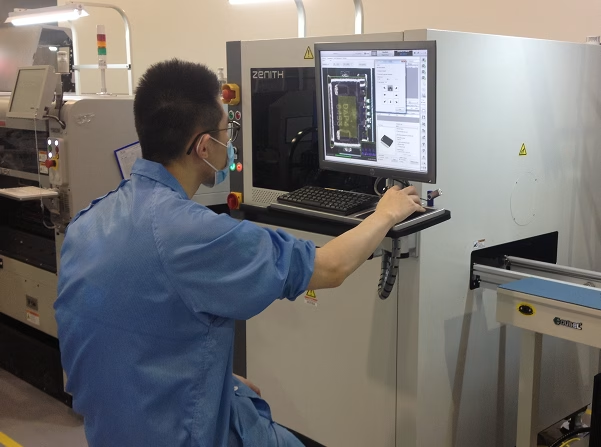
(The workers are using an AOI machine.)
1. What is Automated Optical Inspection (AOI)?
Automated Optical Inspection (AOI) is a machine-vision-based technique used primarily in the manufacturing of printed circuit boards (PCBs) to autonomously scan a board for catastrophic failures and quality defects. It employs sophisticated cameras, lighting systems, and powerful software algorithms to capture detailed images of the PCB and compare them against an approved “golden” board or the design Gerber files. This comparison allows the system to identify deviations that signify potential defects.
Essentially, an AOI system acts as an electronic “eye” that never tires, examining every solder joint, component placement, and trace with meticulous detail. Its primary goal is to ensure that the PCB assembly aligns perfectly with its design specifications and quality standards before moving to the next stage of production or final testing.
2.Why Are AOI Tests Popular
Printed circuit boards (PCBs) serve as a core component underpinning automated optical inspection (AOI) processes.
When placing orders for these boards, any identified errors must be rectified promptly—delays or oversights in this regard could lead to frustrating financial repercussions.
As previously noted, the growing sophistication of modern PCBs has rendered manual inspection methods entirely obsolete.
The industry now pivots toward automated soldering techniques paired with inspection protocols to verify PCB quality. In today’s competitive market landscape, there is a pressing demand for high-volume, premium-grade products that can be delivered to end-users swiftly, all while upholding rigorous quality control standards.
Indeed, automated inspection and testing stand as foundational pillars of an effective electronics testing strategy. By enabling the rapid detection of production defects, these systems play a critical role in accelerating time-to-market for electronic products.
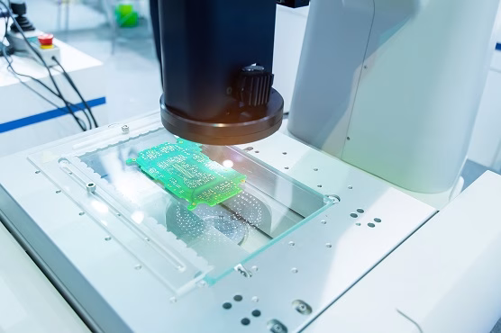
An automated vision system for PCB inspection after assembly.
3.How AOI Works
The operational efficiency of an AOI system hinges on three primary components working in harmony: image acquisition, image processing, and defect analysis.
3.1. Image Acquisition
The process begins with high-resolution cameras capturing multiple images of the PCB. Modern AOI systems often utilize an array of cameras, sometimes including both 2D and 3D capabilities, to capture different perspectives and depths. Specialized lighting, typically LED-based, is crucial here. Various illumination angles and colors are used to highlight specific features and defects, such as solder joint profiles or component markings, by generating contrast. Different lighting conditions can reveal distinct characteristics of the board, making even subtle flaws visible to the system.
3.2. Image Processing and Comparison
Once images are captured, the AOI software processes them rapidly. This involves digital image enhancement techniques to filter noise and sharpen features. The core of the AOI system’s intelligence lies in its ability to compare these acquired images against a set of predetermined criteria. There are generally two main comparison methods:
- Template Matching (Golden Board Comparison):The AOI system is programmed with images of a known-good board (the “golden board”). During inspection, it compares each new board’s image data pixel by pixel, or feature by feature, against this reference. Any significant deviation signals a potential defect.
- Feature-Based Algorithm (CAD Data Comparison):This method utilizes the PCB’s CAD data (Gerber files) to define the expected characteristics of components, traces, and solder joints. The AOI software analyzes features like pad size, component dimensions, and solder paste volume, checking if they fall within acceptable tolerance limits.
3.3. Defect Analysis and Reporting
When a discrepancy is detected, the AOI software flags it as a potential defect. Advanced algorithms classify the type of defect (e.g., missing component, solder bridge, incorrect polarity). The system then presents the flagged areas to an operator for verification. This manual review step is critical to differentiate between actual defects and “false calls” – instances where the AOI misidentifies a normal variation as a fault. Modern AOI systems are increasingly integrating Artificial Intelligence (AI) and Machine Learning (ML) to reduce false calls and improve the accuracy of defect classification, leading to more efficient verification processes.
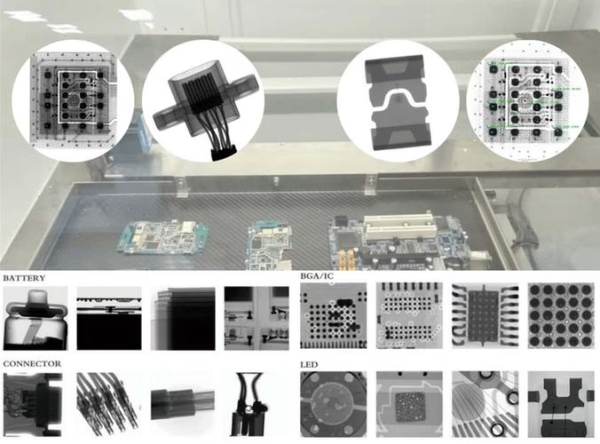
4. Common Defects Detected by AOI
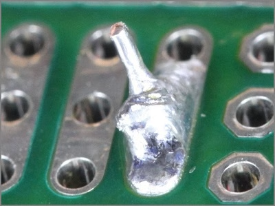
Cold solder joints on the PCB
AOI systems are adept at identifying a wide range of defects that can occur at various stages of PCB assembly. These include both visual and structural anomalies that impact functionality and reliability. Key defects detected include:
- Solder Joint Defects:
-
- Insufficient or excessive solder paste.
- Solder bridges (shorts between pads).
- Open circuits (no solder connection).
- Solder balls or splashes.
- Lifted leads.
- Component Placement Defects:
- Missing components.
- Misaligned or shifted components.
- Wrong components (e.g., incorrect value resistor ).
- Incorrect component polarity (especially critical for diodes, ICs).
- Bent or lifted pins.
- Pad and Trace Defects:
- Scrat ches or damage to traces.
- Contamination or foreign material.
- Etching defects.
- Non-wetting or de-wetting on pads.
This comprehensive detection capability ensures that potential issues are caught early, preventing more expensive repairs or scrap later in the production cycle.
5.The Advantages of AOI Test
Automated Optical Inspection (AOI) has become an indispensable part of PCB manufacturing, thanks to its multiple prominent advantages as follows. It is highly practical for examining PCBs to identify issues including short circuits, line spacing non-compliance, missing solder pads, line width deviations, impacts of high-power loads and frequencies, and excess copper on pads or lines—such inspections are generally carried out after the manufacturing and component assembly stages.
Automated Optical Inspection (AOI) has become an indispensable part of PCB manufacturing, thanks to its multiple prominent advantages as follows:
Versatile Testing Approaches
AOI is mainly applied to post-assembly PCB inspection, where it can identify anomalies or defects like missing components effectively. Additionally, it is also capable of inspecting copper trace irregularities on PCBs right after the manufacturing process.
High Positional Precision
Positional precision is of great significance for optical inspection systems, as PCBs and their components are getting increasingly miniaturized. AOI cameras boast strong performance, which enables them to detect minimal deviations between the captured images and the standard templates—even for the most advanced PCBs.
Programmable Illumination
The illumination system of AOI can be reprogrammed, and different light sources can even be adopted to provide cameras with the optimal view of the PCB surface.
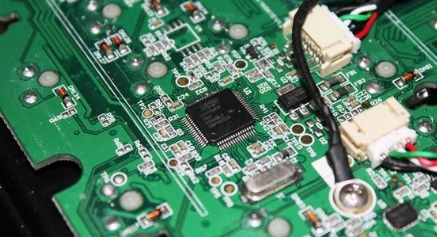
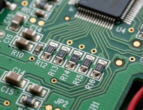
printed circuit board with many electronic components.
Production Cost Reduction
With its high inspection accuracy, AOI helps pinpoint and rectify tiny, imperceptible defects that might incur substantial costs if left unaddressed in the later stages of production.
6.AOI Test Detectable Defects
Automated inspection test systems are capable of identifying a diverse array of errors in printed circuit boards (PCBs). These systems employ various technical approaches to verify whether a PCB meets all predefined quality criteria, with key techniques including template matching, pattern matching, and statistical matching.
Specifically, template matching works by comparing scanned images of the target PCB against a “golden board” (a standard, defect-free PCB). Pattern matching, by contrast, analyzes and contrasts data stored in both flawless and defective systems to pinpoint discrepancies. Statistical matching, meanwhile, leverages statistical datasets to identify and address potential issues that may arise during PCB production.
In addition to these basic methods, advanced visual inspection technologies are also utilized to scan PCBs for manufacturing defects with higher precision.
Fault detection systems further utilize image-based analysis, comparing captured images of PCBs with ideal design diagrams to spot obvious defects efficiently.
- For instance, such systems can effectively detect welding defects, including solder bridges, solder short circuits, solder gaps, excessive solder, irregular solder mass, and open circuits. To mitigate these welding issues, solderability tests provide crucial insights that help enhance the quality of solder joints.
- Component-related defects are also addressed through automated inspection, such as missing components, incorrect component values, misaligned or improperly placed components, faulty parts, and lifted leads. Timely detection of these defects facilitates the prompt correction of errors in PCBs during the manufacturing process.
- Furthermore, ball grid array (BGA) defects—including BGA shorts and open circuit connections—can be detected during automated optical inspection (AOI) tests. These inspections adhere to established industry guidelines and requirements, such as IPC standards, which set forth the quality benchmarks for PCB manufacturing and assembly.
7. What are the Types of AOI Systems?
AOI inspection machines in PCB assembly are primarily categorized as follows:
1) By production line position:
Post-Solder AOI: Installed after the screen printer. Specifically detects solder paste printing quality issues such as paste presence/absence, offset, area, thickness, and short circuits.
Pre-Reflow AOI: Installed after the placement machine and before the reflow oven. Primarily detects defects after component placement, including missing components, misalignment, tombstoning, incorrect part types, physical damage, and polarity errors.
Post-Reflow AOI: This is the most widely used AOI type. It is capable of simultaneously detecting multiple defects arising from the placement and soldering processes. These defects include solder joint shorts, cold solder joints, insufficient solder bridging.
2) By Camera Structure:
Vertical Camera AOI: Camera lens positioned perpendicular to the PCBA board surface.
Tilted Camera AOI: The camera lens is angled to facilitate inspection of component sides and solder joints.
3) By Light Source Type:
Color Lens AOI: Utilizes red, green, and blue light sources with computer-processed color ratios.
Black-and-White Lens AOI: Uses monochromatic light sources with computer-processed grayscale ratios.
4) By Equipment Operation Mode:
In-line AOI: Equipment directly integrated with the production line. PCBA flows continuously through the line, automatically diverted or advanced after inspection. This method offers high efficiency, suits mass production, and enables fully automated end-to-end inspection.
Off-line AOI: Equipment operates independently. Manual loading of PCBA for inspection is required, followed by manual unloading after inspection. This method offers high flexibility, facilitating focused inspection of specific board types or repaired boards, but efficiency is relatively lower.
5) Classification by Inspection Principle:
2D AOI: Primarily identifies defects through two-dimensional image comparison. This is the most widely used technology, effectively detecting the most common placement and soldering defects.
3D AOI: Combines optical imaging with blue-light laser 3D contour measurement technology to provide volumetric information about solder joints. It offers higher coverage and accuracy for micro-components (e.g., 01005) and complex packages (e.g., BGA), excelling particularly in detecting three-dimensional parameters like joint volume and height.
Laser AOI: It is capable of detecting height information, but it features complex programming and slower speeds. It is currently the most expensive AOI system, but offers the highest reliability and precision, even detecting voids within solder joints.
8.Comparison of AOI with Other Inspection Methods
Currently, inspection technologies applicable to PCB assembly can be primarily categorized into: Automated Optical Inspection (AOI), Automated X-ray Inspection (AXI), In-Circuit Testing (ICT), Flying Probe Testing, and Functional Testing (FT). Among these, AOI is the only technology capable of real-time, inline application while simultaneously reflecting trends in SMT process variations. While AOI dominates PCB assembly, each inspection method has distinct advantages, making the choice dependent on specific requirements.
AOI vs. Manual Visual Inspection
AOI operates 5–15 times faster than manual inspection, detecting defects on a board in 10–30 seconds compared to 3–5 minutes for manual inspection. In terms of precision, AOI can detect defects as small as 0.01 mm — ten times finer than manual inspection (0.1 mm) — with a significantly lower error rate. AOI is also more consistent, as it follows pre-set algorithms to ensure uniform standards. Human inspectors, on the other hand, are susceptible to mood and fatigue. However, manual inspection retains cost advantages for small batches and simple PCBA.
AOI vs. X-Ray Inspection
AOI can only detect surface-visible solder joints and is ineffective for joints beneath packages like BGAs or QFPs. X-ray inspection penetrates packaging to reveal internal joint conditions, making it the core technology for detecting internal defects in high-density PCBA (e.g., IC carrier boards). However, X-ray equipment is more costly and operates at relatively slower speeds.
AOI vs. Flying Probe Testing
AOI excels at detecting visual defects like open circuits, short circuits, and component misalignment. Flying probe testing focuses on electrical performance verification, confirming whether an AOI-detected “break” is truly open or a “short” is genuinely conductive. In terms of efficiency, AOI is faster (10-30 seconds per board), while flying probe testing requires 1-2 minutes per board. Typically, AOI is used for rapid screening in mass production, while flying probe testing is employed for sample verification or secondary confirmation of suspected defects identified by AOI.
In a word, AOI technology is merely a tool for fault detection and quality monitoring—not a universal solution for enhancing product quality. One should not expect automatic quality improvement simply by adopting AOI. Only by organically integrating the AOI system into the PCB assembly production and management workflow can the true benefits of this technology be effectively realized.
9.AOI Test Cost
A fully integrated AOI solution starts at a minimum of $30,000, with dual-lane configurations and 3D-enabled systems commanding a notably higher price tag.
It’s important to note that such systems are best suited for high-throughput manufacturing scenarios where circuit boards feature minimal variations in component types and layouts. As a result, investing in this kind of equipment only makes sense if your DIY project truly demands the precision and efficiency that these advanced AOI tools can deliver.
10.Summary
By employing advanced camera systems, sophisticated lighting, and intelligent software, AOI autonomously scans PCBs to detect a wide array of defects—from solder joint imperfections and missing components to incorrect polarity and physical damage. Its ability to perform rapid, consistent, and highly accurate inspections far surpasses the capabilities of manual methods, drastically reducing rework costs, minimizing scrap rates, and improving overall product reliability.
The presence of smaller components and higher densities on contemporary PCB has further prompted the increasing acceptance of automatic checking systems. These facts have been discussed in this article to foster an increased understanding of its role. PCBAndAssembly has advanced detection technology; if you need it, you can contact us in time to get service.
Table of Contents
- 1Què és la inspecció òptica automatitzada (AOI)?
- 2.Per què són populars les proves AOI?
- 3.Com funciona l'AOI
- 4Defectes comuns detectats per AOI
- 5.Els avantatges de la prova AOI
- 6. Prova AOI de defectes detectables
- 7. Quins són els tipus de sistemes AOI?
- 8. Comparació de l'AOI amb altres mètodes d'inspecció
- 9.Cost de la prova AOI
- 10.Summary

Get Your PCB Quote!