How to Optimize PCBA Shielding for EMI Compliance & Performance
The guide explores the principles, methods and practices of PCBA shielding, ensuring optimal performance and regulatory compliance for your electronic designs.
Get Your PCB Quote!
Table of Contents
- 1Apa itu PC?BA Perlindungan dan Mengapa Hal Itu Penting?
- 2Prinsip-prinsip Dasar Perisai EMI/RFI
- 3Jenis-jenis PCBA Solusi Perisai
- 4. Kunci PCBA Bahan Pelindung dan Sifat-Sifatnya
- 5. Pertimbangan Desain Kritis untuk Efektivitas PCBA perisai
- 6Manufaktur dan Pemeliharaan of PCBA Sperlindungan
- 7. Pelindung PCBA FAQ (Pertanyaan Umum)s
- 8. Ringkasan

In our increasingly connected world, electronic devices are everywhere, from the smartphones in our pockets to sophisticated medical equipment and automotive systems. As these devices become more compact and complex, the challenge of ensuring their reliable operation grows. A silent, often invisible threat to performance and longevity is electromagnetic interference (EMI) and radio frequency interference (RFI). This is where PCBA shielding becomes not just beneficial, but absolutely critical.
PCBA shielding is a fundamental aspect of electronic design, meticulously engineered to protect sensitive circuits from unwanted electromagnetic radiation. Without proper shielding, devices can suffer from degraded performance, data corruption, erratic behavior, and even complete failure. This comprehensive guide will explore the principles, methods, and best practices of PCBA shielding, equipping you with the knowledge to ensure optimal performance and regulatory compliance for your electronic designs.
1. What is PCBA Shielding and Why is it Essential?
At its core, PCBA shielding is the practice of enclosing electronic components or entire circuit boards with a conductive barrier. This barrier acts as a protective cage, preventing external electromagnetic fields from interfering with internal circuits and, equally important, containing electromagnetic emissions generated by the device itself. The primary adversaries here are EMI and RFI.
The Silent Threat: EMI and RFI
Electromagnetic Interference (EMI) is any electromagnetic disturbance that interrupts, obstructs, or otherwise degrades or limits the effective performance of electronics. It can be caused by various sources, both natural (like lightning) and man-made (like electric motors, power lines, or even other electronic devices).
Radio Frequency Interference (RFI) is a specific type of EMI that occurs in the radio frequency range. It’s particularly relevant for wireless communication devices, where unwanted signals can disrupt legitimate radio transmissions.
Both EMI and RFI can manifest as noise, corrupting signals and causing malfunctions. In today’s high-speed digital circuits, even tiny amounts of interference can lead to significant problems. For instance, in medical devices, EMI could lead to inaccurate readings, while in automotive electronics, it could compromise safety systems. Regulatory bodies worldwide, like the FCC in the USA and CE in Europe, enforce strict limits on EMI emissions to ensure device compatibility and safety, making effective shielding not just a performance necessity but a legal requirement.
2. Fundamental Principles of EMI/RFI Shielding
Electromagnetic shielding works primarily on two fundamental principles:
1) Reflection
When an electromagnetic wave encounters a conductive barrier, a significant portion of its energy can be reflected away. This phenomenon is most effective when the shield’s material has a high electrical conductivity. The incident wave induces currents in the shield material, and these currents generate opposing electromagnetic fields that reflect the original wave. The effectiveness of reflection is also dependent on the impedance mismatch between the incident wave and the shield material; a greater mismatch leads to more reflection.
2) Absorption
For electromagnetic waves that are not reflected, some energy can be absorbed by the shielding material. This occurs as the wave passes through the conductor, generating eddy currents within the material. The energy of these eddy currents is then dissipated as heat. Materials with good magnetic permeability and electrical conductivity are effective absorbers. Absorption is particularly crucial for lower-frequency magnetic fields, where reflection is less pronounced. The thickness of the shielding material plays a significant role in absorption, with thicker materials generally offering better attenuation.
Effective PCBA shielding often combines both reflection and absorption mechanisms to achieve optimal attenuation of EMI and RFI across a broad spectrum of frequencies.
3. Types of PCBA Shielding Solutions
Shielding solutions can be broadly categorized based on their application level:
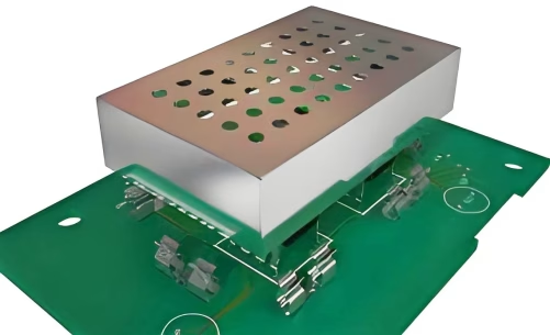
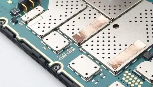
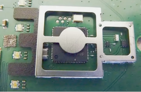
1) Board-Level Shielding
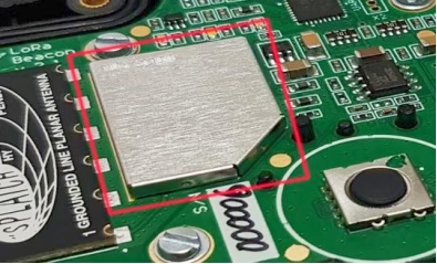
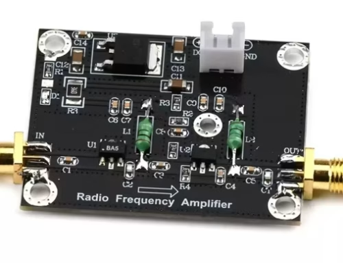
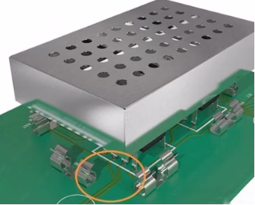
Board-level shielding, also known as on-board shielding, involves placing small, metallic enclosures directly over specific sensitive components or sections of a PCB. These “shielding cans” or “shielding fences” are often made from tin-plated steel, copper alloys, or nickel-silver, and are typically soldered onto the PCB. Their purpose is to isolate specific areas, preventing localized EMI from affecting adjacent circuits or to contain emissions from noisy components. This method is highly effective for critical components like microprocessors, RF modules, or sensitive analog circuits. The design of these shields—including the number of walls, ventilation holes, and corner types—can significantly impact their performance. Multi-cavity shields can isolate several components within a single shield boundary.
2) Enclosure Shielding
Enclosure shielding involves protecting the entire electronic device by housing it within a conductive outer casing. This could be a metal chassis, a plastic enclosure coated with conductive paint, or a combination thereof. The goal is to provide a complete Faraday cage around the entire PCB assembly, preventing EMI/RFI from entering or leaving the system. Gaskets, conductive adhesives, and carefully designed seams are often used to maintain the integrity of the enclosure shield, especially at points where cables enter or leave the device, or where multiple enclosure parts meet. This broader approach is crucial for meeting overall system-level EMI/RFI compliance standards.
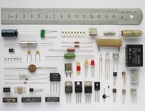
4. Key PCBA Shielding Materials and Their Properties
The choice of PCBA shielding material is paramount to the effectiveness of the EMI/RFI barrier. Different materials offer varying degrees of conductivity, magnetic permeability, corrosion resistance, and cost. Understanding these properties is crucial for selecting the right material for a specific application.
Common PCBA Shielding Materials
The selection process for PCBA shielding materials considers not only electrical properties but also mechanical factors like weight, manufacturability, and environmental durability.
| Material | Key Properties | Common Applications | Notes |
| Copper | Excellent electrical conductivity, good magnetic shielding at high frequencies, highly malleable. | Shielding cans, ground planes, conductive tapes. | Can oxidize; often plated. |
| Aluminum | Lightweight, good electrical conductivity, corrosion resistant. | Enclosures, chassis , EMI gaskets. | Not ideal for low-frequency magnetic fields. |
| Steel (Tin-plated or Nickel-plate) | Good magnetic permeability (especially cold-rolled steel), strong, cost-effective. | Board-level shields, larger enclosures. | Plating enhances conductivity and corrosion resistance. |
| Nickel-Silver | Good electrical conductivity, non-ferrous (non-magnetic), good corrosion resistance, good formability. | Shielding cans, spring contacts. | Often used where magnetic properties are undesirable. |
| Mu-Metal (Nickel-Iron Alloys) | Extremely high magnetic permeability, specifically for low-frequency magnetic fields. | Shielding transformers, sensitive sensors. | Expensive, can lose properties if mishandled (e.g., severe bending). |
| Conductive Plastics | Light weight, allows complex shapes, cost-effective for mass production. | Consumer electronics enclosures. | Achieved by incorporating conductive fillers (carbon, metal fibers/flakes). |
5. Critical Design Considerations for Effective PCBA Shielding
Effective PCBA shielding goes beyond simply placing a metal box over components. It requires careful planning and adherence to specific design principles to maximize attenuation and ensure reliability.
5.1 PCBA Shield Design Parameters & Critical Dimensions
Apertures and Seams: Any opening in a shield (for wires, ventilation, or assembly) acts as an antenna, allowing EMI/RFI to leak in or out. The size, shape, and frequency of these apertures are critical. Smaller, fewer, and strategically placed openings are always better. Seams where shield parts meet must be conductive and continuous to prevent gaps.
Cavity Resonance: Shielding enclosures can act as resonant cavities at certain frequencies, potentially amplifying EMI rather than suppressing it. The dimensions of the shield cavity (length, width, height) determine its resonant frequencies. Designers must ensure these frequencies do not coincide with the operating frequencies of the internal components or external threats. Adding damping materials or breaking up large cavities can mitigate resonance.
Material Thickness: As mentioned, thickness influences absorption. While thicker materials offer better absorption, they also add weight and cost. An optimal balance must be found based on the specific EMI/RFI threats.
Component Placement: The physical layout of components on the PCB significantly impacts shielding effectiveness. Noisy components should be placed far from sensitive ones, and critical traces should be routed to minimize coupling. Shielded components should be strategically placed to maximize the benefit of the shield.
5.2 Grounding Requirements and Methods
Proper grounding is arguably the most crucial aspect of effective EMI /RFI shielding. A shield is only as good as its connection to a solid ground plane. An improperly grounded shield can become an antenna itself, exacerbating interference issues.
1) Single-Point Grounding: Ideal for low-frequency circuits where ground loops are a concern. All ground connections are routed to a single common point.
2) Multi-Point Grounding: More suitable for high-frequency circuits (above 10 MHz) where skin effect and parasitic inductance make single-point grounding ineffective. Multiple connections to a large, low-impedance ground plane are used.
3) Hybrid Grounding: Combines aspects of both, often using single-point grounding for low-frequency signals and multi-point for high-frequency signals.
Grounding Methods for Shields:
Direct Solder Attachment: For board-level shields , soldering the shield walls directly to a dedicated ground trace or plane on the PCB provides a robust, low-impedance connection.
Gaskets and Fingers: For enclosure shielding or removable board-level shields, conductive gaskets (e.g., woven mesh, conductive foam) or spring fingers ensure a continuous electrical connection between shield parts and the ground plane, even with minor misalignments or vibrations.
Chassis Ground: In many systems, the metal chassis serves as the primary ground reference, to which all other shield grounds are ultimately connected.
6. Manufacturing and Maintenance of PCBA Shielding
While design is critical, the manufacturing and ongoing maintenance of PCBA shielding are equally important for long-term performance.
1) Assembly Processes: The method of attaching board-level shields (e.g., soldering, snap-fit) must be precise. Any gaps or imperfect connections during assembly can severely compromise shielding effectiveness. Automated assembly processes often ensure greater consistency.
2) Mechanical Damage: Shields, especially board-level cans, can be susceptible to mechanical damage during handling, testing, or field use. Dents or deformation can create gaps, reduce contact with the ground plane, and degrade shielding performance. Regular inspection is vital, and damaged shields may need replacement or repair.
3) Corrosion: In certain environments, particularly those with high humidity or exposure to corrosive chemicals, PCBA shields can corrode. Corrosion degrades the material’s conductivity, thereby reducing its shielding performance and overall reliability. Proper material selection (e.g., using plated steel or corrosion-resistant alloys) and protective coatings are essential for mitigating this risk.
4) Thermal Management: While often overlooked, shields can trap heat, impacting the thermal performance of enclosed components. Designers must consider thermal pathways, ventilation, and heat dissipation strategies (e.g., thermal vias, heat sinks) to prevent overheating within shielded areas.
7. PCBA Shielding FAQs
EMI (Electromagnetic Interference) is a broad term encompassing any electromagnetic disturbance affecting electronic devices. RFI (Radio Frequency Interference) is a specific type of EMI that occurs within the radio frequency spectrum, often disrupting wireless communication.
Standard plastic enclosures are typically non-conductive and therefore cannot reflect or absorb electromagnetic waves effectively. To make them shield-effective, they must be coated with a conductive material (e.g., conductive paint) or incorporate conductive fillers, essentially turning them into a form of enclosure shielding.
While not every single circuit requires heavy shielding, most modern electronic devices benefit significantly. It’s particularly critical for high-frequency circuits, sensitive analog components, wireless communication modules, and any device that must meet stringent EMI/RFI regulatory compliance standards. Neglecting shielding can lead to unpredictable performance and costly redesigns.
PCBA Shielding should be considered as early as possible in the design phase. Integrating EMC considerations from the start is far more effective and cost-efficient than trying to fix problems later.
Yes, conductive paints and coatings (often containing nickel, copper, or silver particles) can provide effective EMI shielding, especially for plastic enclosures where a metallic housing isn’t feasible. Their effectiveness depends on thickness and conductivity.
Proper grounding is integral to PCBA shielding. A shield needs a low-impedance path to ground to effectively drain away induced currents and reflect electromagnetic waves. Poor grounding can render even the best shielding material ineffective.
8. Summary
PCBA shielding is a cornerstone of reliable electronic design, offering vital protection against the pervasive threats of EMI and RFI. By understanding the fundamental principles of reflection and absorption, choosing appropriate materials like copper or steel, and implementing meticulous design considerations such as proper grounding and aperture management, engineers can significantly enhance device performance and ensure regulatory compliance. From board-level cans isolating sensitive components to full enclosure shielding, each solution plays a critical role. Given the increasing density and speed of modern electronics, embracing robust shielding practices is not just a best practice, but an absolute necessity for optimal functionality and longevity.
Table of Contents
- 1Apa itu PC?BA Perlindungan dan Mengapa Hal Itu Penting?
- 2Prinsip-prinsip Dasar Perisai EMI/RFI
- 3Jenis-jenis PCBA Solusi Perisai
- 4. Kunci PCBA Bahan Pelindung dan Sifat-Sifatnya
- 5. Pertimbangan Desain Kritis untuk Efektivitas PCBA perisai
- 6Manufaktur dan Pemeliharaan of PCBA Sperlindungan
- 7. Pelindung PCBA FAQ (Pertanyaan Umum)s
- 8. Ringkasan

Get Your PCB Quote!