How to Prevent PCB Delamination: Material Selection & design
Understand PCB delamination–what it is, its causes, detection methods, and prevention strategies to ensure the reliability of your electronic devices.
Get Your PCB Quote!

In the intricate world of electronics, Printed Circuit Boards (PCBs) are the unsung heroes, forming the backbone of virtually every device we use, from smartphones to industrial machinery. Their reliability is paramount, as a single flaw can cascade into catastrophic system failures. Among the most insidious and critical issues affecting PCB integrity is delamination—a term that sends shivers down the spine of any electronics engineer or manufacturer. This defect, often hidden from plain sight until it’s too late, compromises both the mechanical strength and electrical performance of a board, potentially leading to costly rejections and reduced product lifespan.
This comprehensive guide aims to demystify PCB delamination. We’ll delve into what it is, explore its root causes, discuss effective detection methods, and outline crucial prevention strategies. By understanding these fundamentals, designers, manufacturers, and quality assurance professionals can take proactive steps to ensure the robustness and durability of their PCB designs, ultimately enhancing the reliability of modern electronics.
1. What is PCB Delamination?
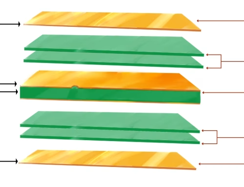
At its core, PCB delamination refers to the undesirable separation of layers within a printed circuit board. PCBs are constructed from multiple thin layers of conductive copper foil and insulating dielectric substrate (often fiberglass impregnated with resin, known as prepreg), all pressed and bonded together under heat and pressure. Delamination occurs when the adhesive bonds between these layers break down, causing them to peel apart. This can happen in several critical areas:
- Between the Copper Foil and Dielectric Substrate:This is a common form, where the conductive traces separate from the insulating material.
- Between Inner Laminate Layers:In multi-layer PCBs, separation can occur between any of the internal prepreg and core layers.
- Between Prepreg and Core:The pre-impregnated material failing to bond properly with the solid core layers.
The visual manifestation of delamination often includes small, visible gaps, bubbles, or blisters on the board’s surface. These ‘blisters’ are essentially pockets of air or moisture trapped between separated layers. Even microscopic separations can compromise the board’s structural integrity and electrical functionality. The consequences range from signal loss and intermittent connections to complete circuit failure, impacting the overall performance and reliability of the electronic device.
2. Common Causes of PCB Delamination
PCB delamination is a multifaceted issue, often stemming from a combination of factors related to materials, manufacturing processes, and environmental stresses. Understanding these causes is crucial for effective prevention.
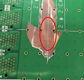
2.1 Thermal Stress
Bubbling and delamination appear on the PCB surface
One of the most significant contributors to delamination is thermal stress, particularly during PCB manufacturing and PCB assembly processes. The rapid heating and cooling cycles that PCBs undergo can put immense strain on the laminated layers. Key thermal events include:
- Soldering Processes: Reflow soldering and wave soldering expose PCBs to high temperatures. If the temperature profile is too aggressive or prolonged, the different coefficients of thermal expansion (CTE) between materials (copper, resin, fiberglass) can cause them to expand and contract at different rates, leading to shear stress and bond failure.
- High Operating Temperatures:Even during normal operation, if a device generates excessive heat, continuous thermal cycling can degrade the adhesion over time, especially in high-power applications.
- Moisture Vaporization:Trapped moisture within the laminate layers can turn into steam at high temperatures, exerting pressure that physically forces the layers apart. This is a common mechanism for blistering.
2.2 Moisture Absorption
Moisture is a silent saboteur of PCBs. The dielectric materials used in PCBs are often hygroscopic, meaning they can absorb moisture from the surrounding environment. If a board with absorbed moisture is subjected to high temperatures (e.g., during soldering), the trapped water rapidly vaporizes into steam. This steam creates internal pressure that can physically push the laminate layers apart, leading to blistering and delamination. Proper storage and pre-baking processes are essential to mitigate this risk.
2.3 Material Issues
The quality and compatibility of materials play a critical role in preventing delamination:
- Poor Adhesive Quality:The prepreg resins used to bond layers must have sufficient adhesion strength. Inferior quality resins or improper resin flow during lamination can result in weak bonds.
- Incompatible Materials:Mixing materials with significantly different CTEs can exacerbate thermal stress issues.
- Low Glass Transition Temperature (Tg):Tg is the temperature at which the resin transitions from a rigid glassy state to a more pliable rubbery state. If the PCB is exposed to temperatures above its Tg during manufacturing or operation, the material can become softer, making the bonds more susceptible to separation. Selecting materials with appropriate Tg values for the application is vital.
2.4 Manufacturing Defects and Process Control
Errors or inconsistencies during the manufacturing and assembly stages can directly lead to delamination:
- Improper Lamination Parameters:Incorrect pressure, temperature, or curing times during the lamination process can result in incomplete resin polymerization or insufficient bonding between layers.
- Aggressive Drilling :Drilling through multiple layers can create localized stress and heat, potentially weakening the surrounding bonds.
- Poor Surface Preparation:Inadequate cleaning or preparation of copper surfaces before lamination can hinder proper adhesion.
- Substrate Damage:Mechanical damage during handling or processing can initiate cracks that propagate into delamination.
While it is common for circuit boards to have some degree of delamination in certain areas, extensive delamination must be avoided. This requires careful consideration of materials, reflow profile, pre-bake settings, and laminate storage to ensure proper matching.
3. Detecting Delamination: Signs and Methods
Early detection of PCB delamination is critical to prevent product failures and minimize costs. Delamination can be insidious, often not immediately visible during standard inspections. However, several methods exist , ranging from basic visual checks to advanced analytical techniques.
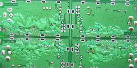
3.1 Visual Inspection
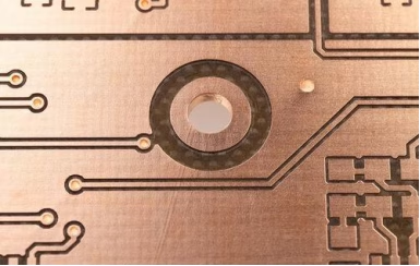
localized PCB blistering
The most straightforward detection method involves a careful visual examination of the PCB. Technicians look for tell-tale signs such as:
- Blisters or Bubbles:These are localized swellings on the board surface, indicating trapped gas (often steam from moisture) that has pushed layers apart. These are frequently referred to as blistering.
- Swelling or Warping:Distortions in the board’s flatness can indicate internal stress and separation.
- Discoloration:Changes in color, particularly around vias or pads, might suggest thermal damage or internal separation.
- Visible Gaps or Cracks:In severe cases, macroscopic gaps between layers or cracks in the laminate material may be evident.
3.2 Micro-Sectioning
For a more definitive internal view, micro-sectioning involves cutting a cross-section of the PCB, polishing it, and examining it under a high-powered microscope. This allows engineers to directly observe the internal layers and identify any separations, voids, or cracks that are not visible externally. It’s a destructive but highly effective method for failure analysis.
3.3 Scanning Acoustic Microscopy (SAM)
SAM is a non-destructive testing technique widely used to detect internal defects, including delamination, voids, and cracks. It works by sending high-frequency ultrasonic waves into the PCB and analyzing the reflected signals. Changes in acoustic impedance at the interfaces between layers (e .g., where a delamination exists) produce distinct echoes, allowing for a detailed mapping of internal structures and the identification of separated areas without damaging the board.
3.4 Thermal Cycling/Shock Testing
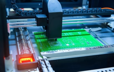
Automated equipment quality inspection
While primarily a reliability test, thermal cycling can also reveal latent delamination. By subjecting PCBs to rapid and repeated changes in temperature, engineers can accelerate the stresses that cause delamination. Boards that survive these tests without delaminating are generally considered more robust. If delamination occurs during such tests, it indicates a design or manufacturing flaw.
4. The Impact of Delamination on PCB Performance
The effects of PCB delamination extend far beyond a cosmetic flaw; they can severely compromise the functionality and longevity of electronic devices. Understanding these impacts underscores why prevention is so crucial:
- Compromised Electrical Performance:Delamination can lead to signal loss, increased impedance, and cross-talk between traces as the dielectric constant changes or traces are physically displaced. This directly affects signal integrity, leading to erratic circuit behavior or complete functional failure.
- Open Circuits and Intermittent Connections:When the copper foil separates from the dielectric, it can break electrical pathways, creating open circuits. Even minor delamination can lead to intermittent connections, which are notoriously difficult to diagnose and troubleshoot.
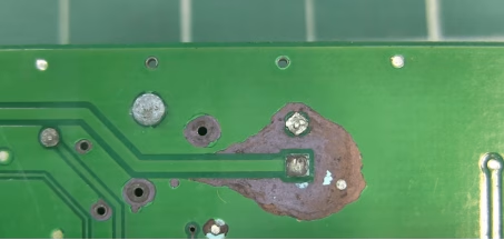
(PCB copper foil delamination occurred)
- Reduced Mechanical Strength:The structural integrity of the PCB is compromised, making it more susceptible to damage from vibration, shock, or bending. This is particularly critical in applications requiring high mechanical reliability, such as aerospace or automotive electronics.
- Increased Risk of Catastrophic Failure:Delamination can expose internal circuitry to environmental factors like moisture and contaminants, leading to corrosion or short circuits. In high-power applications, localized delamination can cause overheating and potential burn-out.
- Decreased Product Lifespan:Boards suffering from delamination are prone to premature failure, reducing the overall lifespan of the electronic product and leading to higher warranty costs and customer dissatisfaction.
These issues may not be immediately visible during standard inspections, yet their effects can ripple across a product’s lifetime. In a world where reliability is non-negotiable, especially for industries like aerospace, automotive, and medical devices, understanding these problems and how to solve them has become critical.
5. Strategies for Preventing PCB Delamination
Prevention is always better than cure, especially when it comes to PCB reliability. A holistic approach, encompassing design, material selection, manufacturing processes, and quality control, is essential to mitigate the risks of delamination.
5.1 Material Selection
- HighTg Laminates: Choose laminate materials with a glass transition temperature (Tg) significantly higher than the maximum temperature the PCB will experience during assembly (e.g., reflow) and operation.
- Matched CTEs:Select materials with similar Coefficients of Thermal Expansion (CTE) to minimize stress build-up during temperature fluctuations.
- Low Moisture Absorption:Opt for materials with low moisture absorption rates, especially for applications in humid environments or those undergoing high-temperature processing.
5.2 Optimized Manufacturing Processes
- Controlled Reflow Profiles:Carefully calibrate reflow oven temperature profiles to ensure proper soldering without exposing the board to excessive heat or prolonged dwell times. The reflow profile should be optimized for the specific materials and components used.
- Proper Pre-Baking:Before assembly, PCBs should be pre-baked (or “dry baked”) to remove any absorbed moisture. This is a critical step, especially for boards that have been stored for extended periods or in humid conditions.
- Optimal Lamination Parameters:During PCB fabrication, strict control over lamination pressure, temperature, and curing cycles is necessary to ensure robust interlayer adhesion.
- Careful Handling:Minimize mechanical stress during all stages of manufacturing, from handling raw materials to final assembly.
5.3 Design Considerations
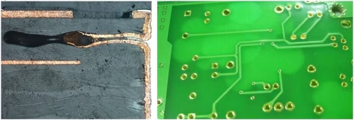
PCB micro-section analysis and surface thermal distribution
- Balanced Copper Distribution:Distribute copper evenly across all layers to prevent localized hot spots and uneven thermal expansion.
- Via Design:Ensure proper via plating and aspect ratios to avoid stress concentrations around barrel walls, which can initiate delamination during thermal cycling.
5.4 Quality Control and Testing
- Incoming Material Inspection:Verify the quality of raw materials (laminates, prepregs, copper foils) before they enter production.
- In-Process Monitoring:Implement continuous monitoring of temperature, pressure, and time parameters during lamination and assembly.
- Regular Testing:Conduct routine reliability tests such as thermal cycling, humidity testing, and periodic micro-sectioning to validate the manufacturing process and material performance.
Addressing PCB delamination requires a comprehensive approach involving design, materials, manufacturing processes, inspection, and failure analysis.
6. PCB Delamination FAQs
While minor, localized delamination in non-critical areas might sometimes be tolerated in less demanding applications, any extensive or propagating delamination is considered a critical defect. It compromises the PCB’s structural and electrical integrity, making it unreliable for most electronic devices, especially in industries where reliability is paramount (e.g., aerospace, medical).
In most cases, repairing a delaminated PCB is not feasible or cost-effective, especially for multi-layer boards where internal separation has occurred. The structural damage is often irreversible without compromising other layers or connections. Prevention through proper design, material selection, and manufacturing processes is almost always the preferred approach.
PCBs, particularly their dielectric materials, can absorb moisture from the environment. When these moist boards are exposed to high temperatures (e.g., during soldering), the trapped moisture rapidly turns into steam. This steam creates significant internal pressure, which can physically force the laminated layers apart, resulting in visible bubbles or “blisters” on the board’s surface.
7. Summary
PCB delamination is a serious reliability issue characterized by the separation of layers within a printed circuit board. This defect, often triggered by thermal stress, moisture absorption, material incompatibilities, or manufacturing flaws, compromises both the mechanical strength and electrical performance of the board. Symptoms can range from visible blisters and warping to invisible internal separations that degrade signal integrity and lead to circuit failures. Effective prevention requires a multi-faceted approach, encompassing careful material selection (high Tg, matched CTEs), optimized manufacturing processes (controlled reflow, pre-baking, proper lamination), intelligent design considerations, and stringent quality control. By understanding and addressing the root causes, manufacturers can significantly enhance the durability and long-term reliability of their electronic products.
Key Takeaways
- PCB delamination is the separation of layers, primarily copper foil and dielectric substrate, compromising board integrity.
- Major causes include thermal stress from soldering, moisture absorption (leading to blistering), and poor material selection or manufacturing process control.
- Detection ranges from visual inspection for blisters and warping to advanced techniques like micro-sectioning and Scanning Acoustic Microscopy (SAM).
- Delamination severely impacts electrical performance, leading to signal loss, open circuits, reduced mechanical strength, and decreased product lifespan.
- Prevention is key, involving high-Tg laminates, optimized reflow profiles, proper pre-baking, and robust quality control throughout the manufacturing process.

Get Your PCB Quote!