Mastering 6-Layer PCB Stackup: Design, Performance & Cost
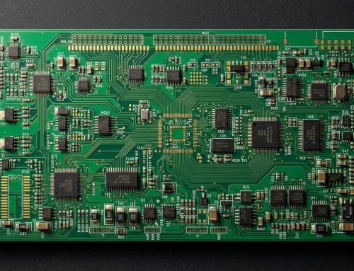
A 6-layer PCB is a multilayer circuit board with six layers of conductive material separated by insulating layers. PCBAndAssembly offers expert PCB assembly services, ensuring that your 6-layer PCBs are manufactured to the highest standards for optimal performance.
Get Your PCB Quote!
Table of Contents

1. Introduction to 6-Layer PCB Stackup
As electronic devices become increasingly sophisticated and demand higher performance, the complexity of Printed Circuit Boards (PCBs) must evolve. Engineers often find themselves hitting the limits of simpler board designs, particularly when it comes to signal integrity and electromagnetic compatibility (EMC). This is where the 6-layer PCB stackup emerges as a versatile and popular solution.
Transitioning from a 4-layer board to a 6-layer board significantly expands design possibilities. The additional layers provide more room for complex signal routing, dedicated ground and power planes, and enhanced control over electromagnetic interference (EMI). A well-designed 6-layer stack up can dramatically improve a board’s electrical performance, reduce crosstalk, and ensure overall reliability, making it an ideal choice for advanced electronic applications. This guide will delve into the specifics of 6-layer PCB stackups, exploring their advantages, optimal configurations , critical design guidelines, and practical applications.
2. What is a PCB Stackup?
Before diving into the specifics of a 6-layer design, it’s essential to understand the fundamental concept of a PCB stackup. A PCB stackup refers to the arrangement of copper layers and insulating materials (dielectrics) that form the structure of a printed circuit board. This layered construction is crucial for dictating the electrical performance, signal integrity ( SI), and electromagnetic compatibility (EMC) of the PCB.
Each layer serves a specific purpose, whether it’s for routing signals, distributing power, or providing a stable ground reference. The choice of materials , their thickness, and their sequence in the stackup directly impact impedance control, crosstalk, and the board’s ability to mitigate EMI. A thoughtful PCB stackup design can minimize noise, improve signal quality, and enhance the overall reliability and performance of the electronic device it powers. Common materials used include FR-4, which is a glass-reinforced epoxy laminate, as well as specialized materials like Rogers or PTFE for high-frequency applications.
3. Why Choose a 6 -Layer PCB?
The decision to graduate from a 4-layer to a 6-layer PCB stackup is often driven by performance requirements that a simpler board cannot meet. While a 4-layer board might suffice for many basic applications, more complex designs with higher clock speeds, denser component placement, or strict noise requirements will benefit significantly from additional layers. Here are several compelling reasons to opt for a 6-layer board:
- Enhanced Signal Integrity:With more layers, designers can create dedicated signal layers separated by solid ground planes. This isolation helps to reduce crosstalk between high-speed signals and ensures cleaner signal transmission.
- Improved EMI/EMC Performance :A 6-layer stackup allows for more effective shielding of sensitive signals by sandwiching them between ground or power planes. This configuration significantly reduces electromagnetic interference (EMI) both emitted by and susceptible to the board, crucial for meeting regulatory compliance.
- Better Power Distribution Network (PDN):Dedicated power and ground planes provide a low-impedance path for current return, which is vital for stable power delivery to components, especially integrated circuits (ICs) and FPGAs. This helps mitigate power integrity (PI) issues.
- Greater Routing Flexibility:The additional layers provide more “real estate” for routing traces, enabling designers to manage complex interconnections more efficiently. This can be particularly beneficial for boards with high pin-count components or dense layouts.
- Cost-Effectiveness for Performance:While more expensive than a 4-layer board, a 6-layer PCB offers a good compromise between complexity, performance, and cost when compared to 8-layer or higher count boards. It delivers a significant performance boost without the substantial cost increase associated with very high layer counts.
Ultimately, a 6 -layer PCB stackup strikes a balance, providing the necessary complexity and performance for modern electronic applications that require more routing flexibility, better signal integrity, and superior EMI reduction than a 4-layer board can offer.
4. Optimal 6-Layer PCB Stackup Configurations
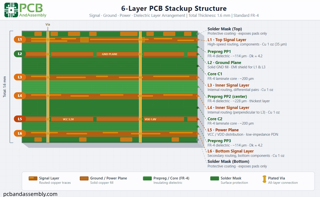
The arrangement of layers in a 6-layer PCB stackup is critical for its electrical performance. While there are various ways to configure the layers, some designs are inherently better for signal integrity and EMI reduction than others. A common principle is to provide solid ground or power planes adjacent to signal layers to provide clear return paths and shielding.

Recommended 6-Layer Stackup Example: Signal- Ground-Signal-Power-Ground-Signal
One of the most widely recommended and balanced 6-layer PCB stackup configurations is illustrated below. This arrangement prioritizes strong signal integrity and effective EMI management:
| Layer | Type | Function/Benefit |
| Layer 1 (Top) | Signal | Primary high-speed signal routing, component placement. Provides excellent reference to Layer 2 ( Ground). |
| Layer 2 | Ground | Solid ground plane for Layer 1. Provides shielding and a clear return path. |
| Layer 3 | Signal | Inner signal layer , often for less critical signals or differential pairs. Referenced to Layer 2 (Ground) or Layer 4 (Power). |
| Layer 4 | Power | Dedicated power plane. Provides stable voltage distribution and acts as a shield. |
| Layer 5 | Ground | Solid ground plane for Layer 6 and return path for Layer 4. Crucial for EMI reduction. |
| Layer 6 ( Bottom) | Signal | Secondary signal layer, often for less critical signals or routing that couldn’t fit on the top layer. Referenced to Layer 5 (Ground). |
This configuration excels because :
- Each signal layer (1, 3, 6) is adjacent to a solid plane (ground or power), providing a low-impedance return path for signals and good impedance control.
- The inner signal layer (Layer 3) is sandwiched between two planes, offering excellent shielding.
- The power and ground planes (Layers 4 & 5) are adjacent, forming a tight coupling that provides effective decoupling and reduces noise in the power distribution network.
Less Ideal Stackup (to avoid for high-speed designs): Signal-Power-Signal-Signal-Ground-Signal
A stackup like “SIG/PWR/SIG/SIG/GND/SIG” is generally considered poor from an EMC perspective and is likely only appropriate for very low-speed or DC applications. The main issues arise from:
- Lack of consistent ground planes adjacent to signal layers, leading to uncontrolled impedance and poor return paths.
- Signal layers not being adequately shielded, increasing the risk of crosstalk and EMI.
Understanding these optimal configurations versus problematic ones is a cornerstone of effective 6-layer PCB design guidelines, significantly influencing a board’s performance and reliability.
Alternative Configuration 2: SIG/GND/SIG/SIG/PWR/GND (Routing-Density Priority)
This arrangement prioritizes routing density over optimal signal integrity. Two adjacent internal signal layers (L3 and L4) significantly increase routing capacity, making it suitable for dense designs with moderate speed requirements. The trade-off is reduced shielding between L3 and L4, since they share no intervening ground plane. This configuration is best used when you need maximum routing channels and signal speeds are below the GHz range where tight shielding is critical.
Alternative Configuration 3: SIG/GND/SIG/GND/PWR/SIG (Maximum Signal Integrity)
This is the premium configuration for signal integrity. By using two dedicated ground planes (L2 and L4), every signal layer has an adjacent solid ground reference, ensuring tightly controlled impedance and excellent EMC performance throughout. The cost is one fewer signal routing layer compared to Configuration 1. This stackup is ideal for GHz-level designs, RF sections, or any application where EMC compliance is the top priority. Engineers sacrifice routing flexibility to gain optimal electrical performance.
5. Key Design Considerations for 6-Layer PCBs
Designing a 6-layer PCB involves more than just adding layers; it requires careful consideration of several critical factors to maximize performance and avoid common pitfalls. These considerations are fundamental to achieving robust signal integrity, power integrity, and electromagnetic compatibility.
Signal Integrity (SI)
With high-speed signals, maintaining signal integrity is paramount. This involves:
- Impedance Control:Traces on signal layers must maintain a consistent characteristic impedance (typically 50 ohms for single-ended signals, 100 ohms for differential pairs). This is achieved by carefully controlling trace width, dielectric thickness, and the dielectric constant of the material (e.g., FR-4).
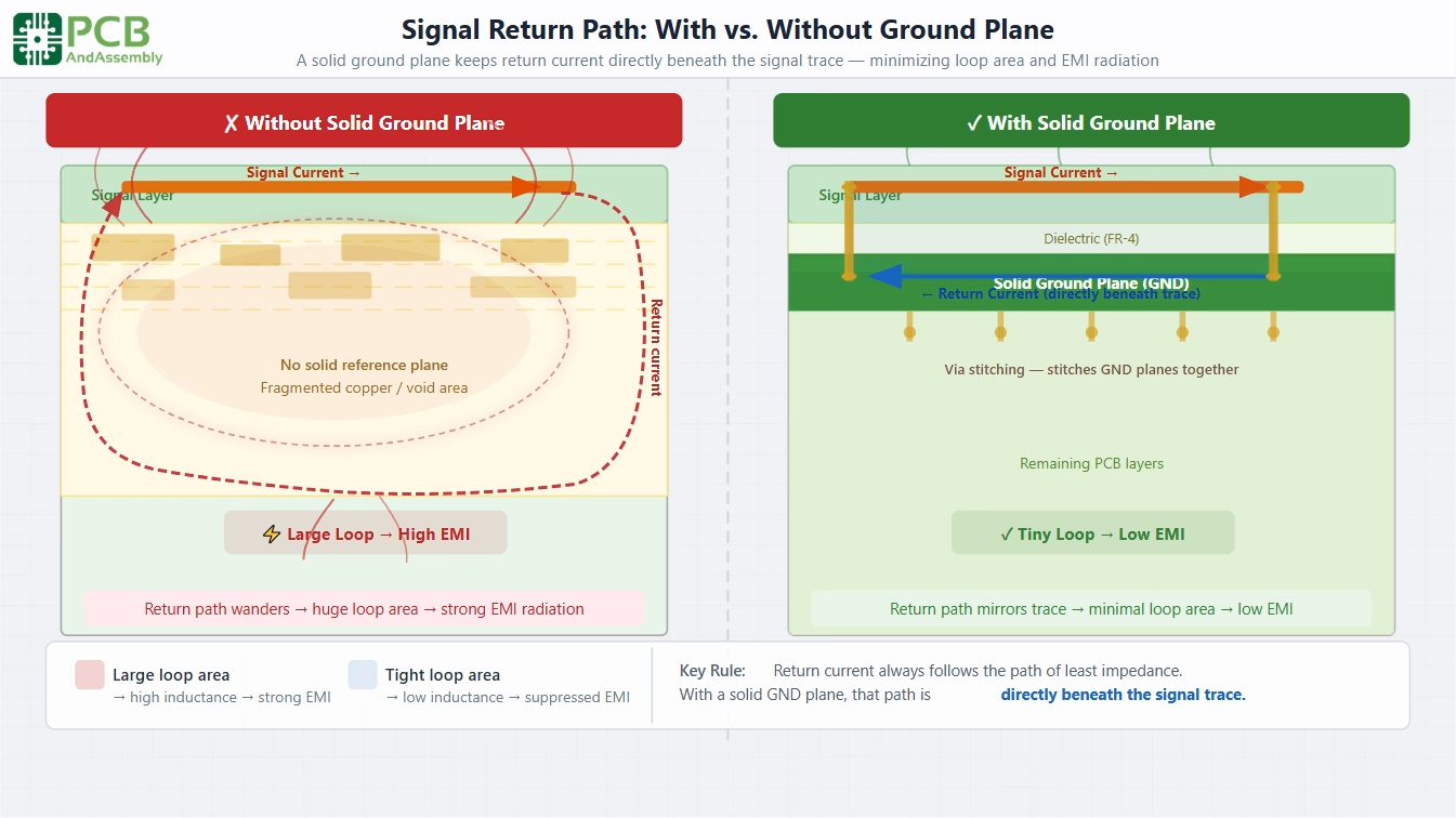
- Crosstalk Reduction:Placing signal layers adjacent to solid ground planes minimizes inductive and capacitive coupling between adjacent traces. Strategic routing, such as maintaining adequate spacing between traces and avoiding long parallel runs, also helps.
- Return Paths:Ensuring a clear, unbroken return path for signals directly beneath the trace is crucial. Vias should be planned to provide direct return paths to ground planes, especially when signals switch layers.
Power Integrity (PI )
A stable power distribution network (PDN) is essential for reliable operation:
- Decoupling Capacitors:Proper placement and sizing of decoupling capacitors are vital for filtering noise and providing instantaneous current to active components. Placing them close to component power pins is a common best practice.
- Plane Proximity:Keeping power and ground planes tightly coupled (thin dielectric between them) creates a large parasitic capacitance, which is effective in suppressing high-frequency noise and providing a stable power source.
EMI/EMC Reduction
Minimizing electromagnetic interference is a key benefit of multi-layer boards:
- Shielding:Solid ground planes act as shields, containing electromagnetic fields generated by signals and preventing external noise from interfering with internal circuitry.
- Stackup Optimization:As discussed, optimal stackup configurations are designed to provide maximum shielding and minimize radiation.
- Via Stitching:Using vias to “stitch” ground planes together around high-frequency traces or component areas helps to contain electromagnetic fields.
Routing Flexibility and Density
The extra layers provide significant routing advantages:
- Designers can dedicate layers to specific types of signals (e.g., high-speed, low-speed, differential pairs) or power/ground, simplifying routing complexity.
- The increased routing space reduces the need for extensive via usage, which can sometimes degrade signal quality if not properly managed.
Material Selection
The choice of PCB materials significantly impacts performance:
- Dielectric Constant (Dk):For high-frequency applications, materials with a stable and lower Dk are preferred to maintain impedance consistency and reduce signal loss .
- Loss Tangent (Df):Materials with a lower Df reduce signal attenuation, which is important for very high-speed signals. FR-4 is a common and cost-effective choice, but for RF or millimeter-wave applications, specialized materials like Rogers or PTFE may be necessary.
For most 6-layer PCB applications below 3 GHz, standard FR-4 or high-Tg variants perform adequately. The table below summarizes common material choices and their typical performance characteristics:
| Material | Dk (Er) | Df (Loss) | Cost Factor | Best Application |
| Standard FR-4 | 4.2–4.5 | 0.020 | 1x (baseline) | General purpose, ≤1 GHz |
| High-Tg FR-4 | 4.2–4.5 | 0.020 | 1.2x | Lead-free assembly, thermal stress |
| Isola 370HR | 3.9 | 0.009 | 1.5x | High-speed digital, ≤3 GHz |
| Rogers RO4350B | 3.5 | 0.0037 | 3x | RF, microwave, ≥5 GHz |
| Megtron 6 | 3.4 | 0.002 | 4x | Premium high-speed (>10 GHz) |
Via Design and Layer Transitions
Through-hole vias in a 6-layer PCB connect all six layers, which creates stubs for high-speed signals. When running traces above 3 GHz, designers should consider back-drilling to remove unused via barrel sections, or use blind/buried vias to minimize stub effects and signal degradation.
A critical but often overlooked requirement: place a ground return via near every signal via that transitions between layers. This maintains a low-inductance return path and prevents signals from finding unintended routes through the power plane, which can be a major source of EMI radiation.
By meticulously addressing these design considerations, engineers can harness the full potential of a 6-layer PCB stackup to create robust, high-performance electronic products.
6. Applications of 6-Layer PCBs
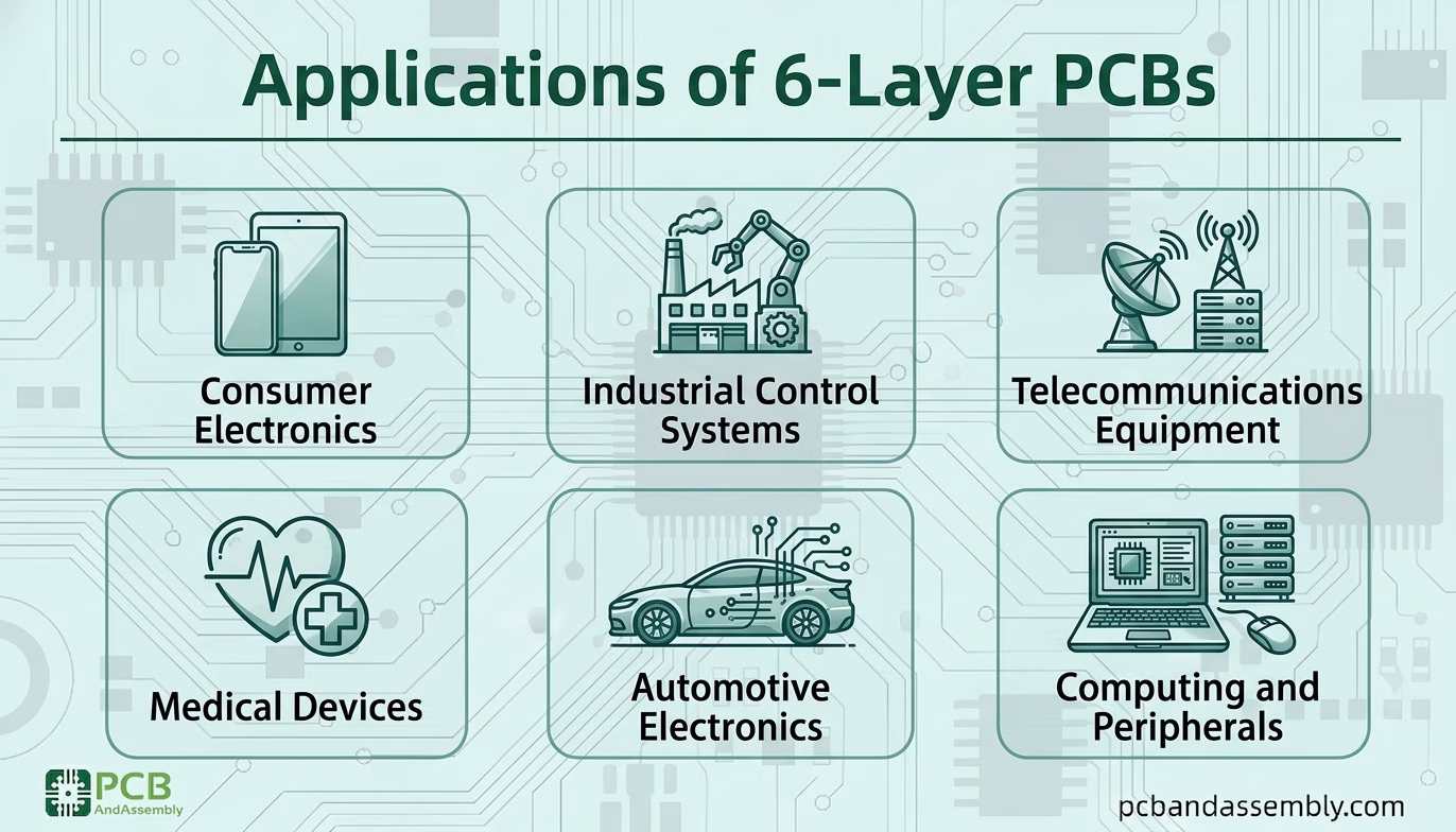
The versatility and balanced performance of 6-layer PCB stackups make them suitable for a wide array of modern electronic applications. They bridge the gap between simpler 4-layer boards and the much higher complexity and cost of 8-layer or more dense designs, offering an optimal blend of features for many mid-to-high complexity products. Some common applications include:
- Consumer Electronics:Devices like smartphones, tablets, high-definition televisions, and advanced gaming consoles often utilize 6-layer PCBs to accommodate complex processors, memory, and various communication interfaces (Wi-Fi, Bluetooth).
- Industrial Control Systems:PLCs (Programmable Logic Controllers), motor drives, and other industrial automation equipment benefit from the enhanced signal integrity and EMI reduction offered by 6-layer boards, ensuring reliable operation in noisy industrial environments.
- Telecommunications Equipment:Routers, switches, base stations, and network interface cards frequently employ 6-layer designs to manage high-speed data transmission, complex signal routing, and stringent EMI requirements.
- Medical Devices:From diagnostic equipment to patient monitoring systems, medical electronics require high reliability and precision. 6-layer PCBs help achieve this by providing stable power distribution and minimizing signal noise.
- Autom otive Electronics:Advanced driver-assistance systems (ADAS), infotainment systems, and engine control units (ECUs) leverage 6-layer boards for their ability to handle complex data, high-speed interfaces, and operate reliably in harsh automotive conditions .
- Computing and Peripherals:Graphics cards, motherboards (for less extreme cases than high-end gaming/server), and embedded computing modules are common areas where 6-layer PCBs offer the necessary performance for modern processors and memory.
These applications underscore the fact that 6-layer PCBs are a versatile and cost-effective solution for designs requiring more than basic functionality, but without the extreme demands that necessitate 8-layer or higher count boards.
7. Cost-Benefit Analysis and Manufacturer Selection
When considering a 6-layer PCB, a thorough cost-benefit analysis is essential. While a 6-layer board will naturally be more expensive than a 4-layer counterpart due to additional materials and manufacturing steps, the enhanced performance often justifies the increased cost. The benefits in terms of improved signal integrity, EMI reduction, and routing flexibility can lead to more reliable products, faster development cycles, and fewer post-production issues, ultimately saving costs in the long run.
The cost difference between a 4-layer and 6-layer board typically includes:
- Additional copper foil and prepreg materials.
- More lamination cycles.
- Increased drilling and plating steps.
- Potentially tighter tolerances for etching and alignment.
For reference, the table below shows typical prototype pricing (5–10 pieces) to give designers a realistic cost baseline when comparing 4-layer and 6-layer options:
| Board Size | 4-Layer Cost | 6-Layer Cost | Typical Increase |
| 50 × 50 mm | $15–$25 | $25–$40 | ~60% |
| 100 × 100 mm | $40–$60 | $65–$100 | ~65% |
| 150 × 100 mm | $70–$90 | $110–$150 | ~57% |
However , the avoided costs of debugging signal integrity issues, re-spins due to EMI failures, or the inability to meet performance targets can far outweigh the initial material and fabrication cost increase. For designs where a 4-layer board is simply insufficient for meeting performance goals, a 6-layer PCB becomes a highly cost-effective solution.
Selecting the Best Manufacturer
Choosing a reliable PCB manufacturer is paramount to ensure the quality and performance of your 6-layer board. Look for manufacturers that offer:
- Experience with Multi-Layer Boards:Ensure they have a proven track record of fabricating 6-layer and higher layer count PCBs.
- Advanced Manufacturing Capabilities:The ability to maintain tight tolerances for trace width, spacing, and drill accuracy is crucial for impedance control and reliability.
- Material Options:A good manufacturer should offer a range of dielectric materials, including various grades of FR-4 and specialized high-frequency laminates, to match your design requirements.
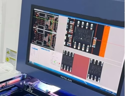
- Quality Control:Robust inspection and testing processes (e.g., flying probe, AOI, electrical testing) are essential to catch defects early.
- Technical Support:A responsive technical team can provide valuable feedback on Design for Manufacturability (DFM) and help optimize your design files (Gerber RS-274 X format is most preferred).
- Cost-Effectiveness:While not the sole factor, competitive pricing coupled with quality is always desirable. Services that offer one-stop solutions for PCB fabrication and assembly can also streamline your workflow.
Many suppliers, such as PCBAndAssembly, offer comprehensive manufacturing solutions and technical support, which can be invaluable for hardware innovators worldwide. Always provide complete design files, including Gerber files , drilling files, and Bill of Materials (BOM) for assembly, to avoid delays and ensure accurate fabrication.
8. 6-Layer PCB Manufacturing Process
Understanding how 6-layer PCBs are manufactured helps designers make better decisions and communicate effectively with fabricators. The process is more complex than 4-layer production due to multiple lamination cycles and stricter alignment requirements.
Step 1: Design and File Preparation
Designers use EDA (Electronic Design Automation) software such as Altium Designer, KiCad, or Eagle to create the schematic and PCB layout. After layout, Gerber files are generated for each layer, including copper traces, drill holes, solder masks, and silkscreen patterns. These files are submitted to the fabrication house for production.
Step 2: Inner Layer Fabrication
The process begins with two double-sided copper-clad laminates (cores). Photoresist is applied to the copper and exposed through a UV mask to define circuit patterns. Chemical etching removes unwanted copper, leaving the desired traces and pads. Automated Optical Inspection (AOI) verifies that the etching has accurately replicated the design before proceeding.
Step 3: Layer Alignment and Lamination
The two processed cores are stacked with prepreg sheets and outer copper foils. Precise alignment using tooling holes ensures layer-to-layer registration within ±3 mils for standard processes. The entire stack is laminated under heat (approximately 175°C) and pressure (300–500 PSI) to create a solid, uniform bond without damaging the inner layers.
Step 4: Drilling and Plating
CNC machines drill precise through-holes for vias and component leads. After drilling, the holes are first coated with a thin electroless copper layer to make them conductive, then built up with electrolytic copper plating to create robust electrical connections across all six layers. The quality of this plating step is critical—poor plating leads to barrel cracks and open circuits in the field.
Step 5: Outer Layer Processing, Surface Finish, and Testing
The outer copper layers are imaged and etched after drilling, allowing drill registration to be verified first. A solder mask is applied to protect traces and prevent solder bridges. Silkscreen markings are printed for component identification. Finally, a surface finish—such as HASL (Hot Air Solder Leveling) or ENIG (Electroless Nickel Immersion Gold)—is applied to the exposed pads. Every finished board undergoes electrical testing (flying probe for prototypes, fixture testing for production volumes) to verify connectivity and catch defects before shipment.
9. Common 6-Layer PCB Design Mistakes to Avoid
Even experienced designers encounter pitfalls when working with 6-layer boards. Being aware of the most frequent errors can save significant time and cost during design review and board bring-up:
- Splitting Reference Planes:Cutting slots in ground planes to route traces disrupts return current paths and creates EMI radiation. Use vias to transition between layers rather than cutting planes.
- Neglecting Return Vias at Layer Transitions:Every signal via that changes layers must have a nearby ground via to provide the return current path. Forgetting this creates loop inductance that radiates at high frequencies.
- Routing High-Speed Signals on the Wrong Layer:Placing differential pairs on internal layers that lack an adjacent solid reference plane undermines impedance control. High-speed signals should be routed on outer layers (L1 and L6) where they are tightly coupled to adjacent ground planes.
- Asymmetric Copper Distribution:An unbalanced stackup—where copper weight or layer arrangement is not symmetric around the board center—causes warping during reflow soldering, making assembly difficult and potentially damaging solder joints.
- Over-Constraining Impedance Tolerances:Specifying ±5% impedance tolerance when ±10% would be perfectly adequate adds manufacturing cost without any real benefit. Match the tolerance specification to actual signal requirements.
10. 6-Layer PCB FAQ
Q1:What is the main advantage of a 6-layer PCB over a 4-layer PCB?
A: The primary advantage is the significantly improved ability to manage signal integrity, reduce EMI, and provide more routing flexibility due to additional dedicated ground and power planes and extra signal layers. This helps in achieving higher performance and reliability for complex electronic designs.
Q2:Can I use a 6-layer PCB for high-frequency applications?
A: Yes , a well-designed 6-layer PCB stackup, particularly with proper impedance control and the right choice of dielectric materials (like low Dk/Df FR-4 or specialized laminates), is often suitable for many high-frequency and RF applications. Its ability to shield signals and provide stable power makes it a strong candidate.
Q3:What types of files are needed to get a 6-layer PCB manufactured?
A: Typically, manufacturers require PCB design files in Gerber RS-274X format, drilling files, and a Bill of Materials (BOM) if assembly services are also needed. It’s often recommended to compress all files into a single .zip or .rar archive.
Q4:How does a 6-layer PCB help with EMI?
A 6-layer PCBs mitigate EMI by allowing for dedicated internal ground and power planes that sandwich signal layers. These planes act as shields, containing electromagnetic fields and providing robust, low-impedance return paths for signals, thereby reducing both emitted and susceptible interference.
Q5:What is the standard thickness of a 6-layer PCB, and what options are available?
A: The industry standard thickness is 1.6 mm (0.063 inches), which provides the best balance of mechanical strength, via aspect ratio, and cost-effectiveness. Thinner options (1.0 mm and 1.2 mm) are available for compact or card-edge connector designs, while thicker options (2.0 mm and 2.4 mm) are used in high-power or mechanically demanding applications. Thinner boards can cost more despite using less material because they require tighter process control and have higher scrap rates.
Q6:Can a 6-layer PCB be repaired if damaged?
A: While a 6-layer PCB can be repaired, the process is significantly more complex than with single or double-sided boards due to the internal layer arrangement. Repairs typically require specialized equipment and skilled technicians. Common repairs include fixing broken surface traces, reworking solder joints, or replacing damaged surface-mount components. Damage to internal layers (such as ground or power planes) is much harder to address and may render a board irreparable in practice, making thorough design review and quality manufacturing essential from the start.
11. Summary
The 6-layer PCB stackup represents a crucial evolutionary step for electronic designers moving beyond the limitations of 4-layer boards. By offering additional dedicated layers for signals, ground, and power, it provides a superior platform for managing complex routing, enhancing signal integrity , and significantly reducing electromagnetic interference. Optimal stackup configurations, such as the Signal-Ground-Signal-Power-Ground-Signal arrangement, are vital for maximizing these benefits, ensuring stable power delivery, and controlling impedance. While the initial cost is higher than a 4-layer board, the performance advantages—leading to greater product reliability and reduced development challenges—often make it a highly cost-effective solution for a wide range of modern applications in consumer electronics, industrial control, telecommunications, and more . Careful design considerations and the selection of a capable manufacturer are key to fully leveraging the power of a 6-layer PCB stackup.
Table of Contents

Get Your PCB Quote!