PCB Solder Bridge Guide: Causes, Prevention & Rework
PCB assembly solder bridge issues are “invisible killer” in electronics manufacturing. Only by knowing their causes, hazards and methods can it be avoided.
Get Your PCB Quote!
Table of Contents
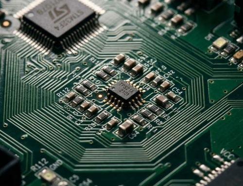
Solder bridge is one of the common defects encountered during PCB assembly, particularly in the SMT (Surface Mount Technology) placement process. The occurrence of solder bridge issues often severely impacts product quality and reliability. Solder bridge can cause short circuits, signal interference, and even lead to product malfunction. Therefore, effectively preventing and avoiding solder bridge problems has become a critical challenge for SMT placement factories.
1. What is Solder Bridge?
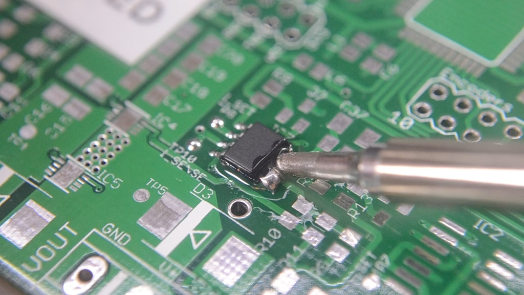
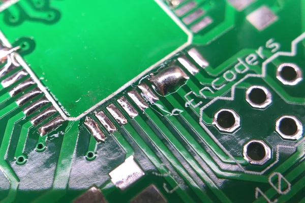
Solder bridge refers to the phenomenon where solder flows at high temperatures during SMT assembly, causing connections between two or more pads and resulting in short circuits. Solder bridge typically leads to the following issues:
Circuit Shorting: Solder flow creates a short circuit between two pads, potentially causing the circuit to malfunction.
Signal Interference: Solder bridges may alter circuit impedance, disrupting signal transmission and compromising device performance.
Product Failure: Severe solder bridge can prevent product startup or cause malfunctions, affecting functionality and stability.
2.Why do Solder Bridge Issues Occur?
Solder bridge is a manufacturing defect in electronic soldering where abnormal solder flow creates unintended conductive paths between adjacent pads. It is crucial to understand that PCB solder bridge is not an “accidental occurrence”; its emergence is closely tied to multiple factors including soldering processes, material selection, and operational standards.
1) Process Parameter Issues
Improper Temperature Control: Excessively rapid reflow oven ramp rates or unscientific temperature profile settings cause excessive solder flow.
Excessive Placement Pressure: Uneven pressure during component placement squeezes solder, forming solder bridges.
2) Equipment and Material Factors
Insufficient Equipment Precision: Examples include stencil registration deviation (exceeding ±0.1μm) or inadequate solder paste printing system accuracy.
Abnormal Material Properties: Low solder paste viscosity or stencil aperture size deviation increases solder flowability.
3) Design Defects
Unreasonable PCB Layout: Insufficient pad spacing, reversed component orientation, or uneven weight distribution causing tilting.
QFN Package Design: Heat sink pad structures prone to solder squeeze, especially with significant height differences between inner and outer row solder joints.
4) Environmental and Operational Factors
Environmental Conditions: Excessive humidity or inadequate cleanliness may compromise soldering quality.
Operational Errors: Such as uneven photoresist coating or incorrect exposure parameter settings.
3. Hazards of Solder Bridge
Solder bridge not only disrupt normal circuit operation but also incur additional production costs. Specific impacts include:
Increased Rework Costs: Once a solder bridge occurs, products require rework and repair, raising production expenses and extending lead times.
Degraded Product Quality: Frequent solder bridge issues diminish product quality, harming the company’s brand reputation and market competitiveness.
Reduced Production Efficiency: Solder bridge problems often cause production line stoppages, leading to missed delivery deadlines and impacting overall manufacturing efficiency.
4. How to Quickly Identify Solder Bridge?
Visual Inspection
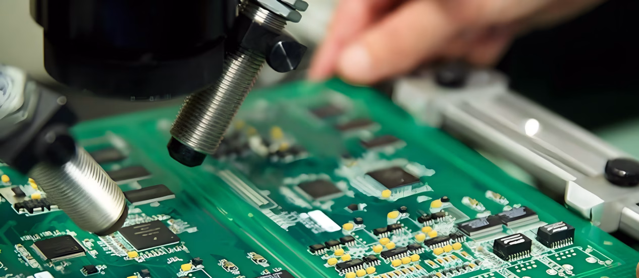
For general users or beginners, start by visually inspecting whether there are any excess solder connections between adjacent solder points. Under good lighting, use a magnifying glass to closely examine densely populated pad areas (e.g., QFPs, header pins). If you observe a distinct solder bridge between two adjacent pads or traces that matches the surrounding solder color, it is likely a solder bridge.
Multimeter Measurement
For hidden solder bridge, a multimeter is required. Set the multimeter to the continuity test mode. Touch both probes to two conductors that should be isolated (e.g., two adjacent pads). If the multimeter emits a beep, it indicates continuity between them, suggesting a potential solder bridge. Use the “cut-and-test method” to isolate sections and progressively narrow down the short-circuit area.
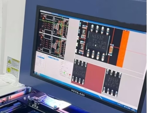
AOI/X-Ray Inspection
For mass-produced PCB assembly, manufacturers employ “AOI (Automated Optical Inspection) equipment.” This technology captures high-resolution images of the PCB and compares them against standard reference images, rapidly identifying defects such as solder bridge, cold solder joints, and missing components with detection accuracy down to 0.01mm.
X-Ray inspection utilizes grayscale contrast to detect solder bridge in hidden solder joints like BGAs, allowing observation of abnormal solder distribution.
5. How to Prevent Solder Bridge Issues?
Solder bridge is one of the most common and severe defects in PCB assembly. It not only compromises circuit board functionality but also incurs additional rework costs and production downtime. To prevent solder bridge, meticulous planning and optimization are required at every stage from PCB design to manufacturing processes.
1) Optimize PCB Design
Sound PCB design is the first step in preventing solder bridge. Through rational circuit board layout and component placement, bridging incidents can be significantly reduced.
Optimize Component Placement: During design, ensure components are arranged logically. Avoid clustering large, heavy components on one side to prevent PCB warping. Distribute component weight evenly using gradient layouts and increase vent hole distribution to maintain PCB balance.
Increase Pad Spacing: Utilize trailing pads (for spacings <0.2mm) or solder-stealing pads (for spacings <1.27mm), guiding solder flow via extended lines or additional pads. To prevent excessive solder migration, maximize spacing between pads during design. Adequate pad spacing effectively restricts solder flow at high temperatures, reducing solder bridge probability.
Set Reasonable Solder Mask: Consider adding solder mask around pads during design, precisely controlling mask aperture dimensions to restrict solder flow areas. This prevents solder overflow and lowers solder bridge risks.
2) Properly Set the Reflow Oven Temperature Profile
The temperature profile of the reflow oven significantly impacts solder paste flowability. A well-designed profile controls the solder melting process, preventing excessive paste flow.
Gradual Heating: Maintain a gradual upward trend in the reflow temperature profile to prevent excessive temperatures that could cause overly aggressive solder activity.
Appropriate Cooling Rate: The cooling phase of reflow soldering also requires careful control. Excessively rapid cooling can lead to uneven solder solidification, resulting in poor joint quality and increased solder bridge.
3) Optimize Solder Paste Printing Process
The quality of solder paste printing directly impacts solder bridge issues during the soldering process. A well-designed solder paste printing process effectively controls solder volume and distribution, thereby reducing solder bridge risks.
Selecting the Right Solder Paste Printer: Replace stencils with solder paste printers. Modern printers precisely control paste volume without relying on stencil apertures, eliminating uneven paste coverage caused by improper stencil openings or warping.
Controlling Solder Paste Volume: In actual production, solder paste volume should be reasonably controlled to prevent excessive flowability, which can cause solder bridge.
4) Appropriate Placement Pressure and Component Positioning
During the SMT placement process, correct component positioning and proper placement pressure settings are crucial factors in preventing solder bridge.
Correct Component Positioning: Ensure components are placed in the correct orientation and precise location during placement to prevent uneven solder flow and subsequent solder bridge caused by improper placement.
Controlling Placement Pressure: Appropriately control placement pressure to avoid component displacement or excessive solder flow due to pressure that is either too high or too low.
5) Materials and Environment
Flux Selection: Use highly active flux to enhance wettability.
Environmental Control: Maintain a clean production environment and avoid excessive humidity.
Equipment Maintenance: Regularly clean the stencil and inspect the stability of the reflow oven temperature.
6) Appropriate Manual Inspection and Rework
Even with thorough design and process measures to prevent bridging, minor bridging issues may still occur during production. In such cases, timely detection and rework through manual inspection serve as a crucial supplementary measure to prevent solder bridge issues from compromising product quality.
Solder Joint Inspection: Utilize AOI (Automated Optical Inspection) and manual inspection to monitor defects in real-time, promptly identify solder bridge issues, and prevent defective products from advancing to subsequent processes.
Rework Procedures: For existing solder bridge issues, employ rework methods such as laser cutting or microwave treatment to ensure product quality meets specifications.
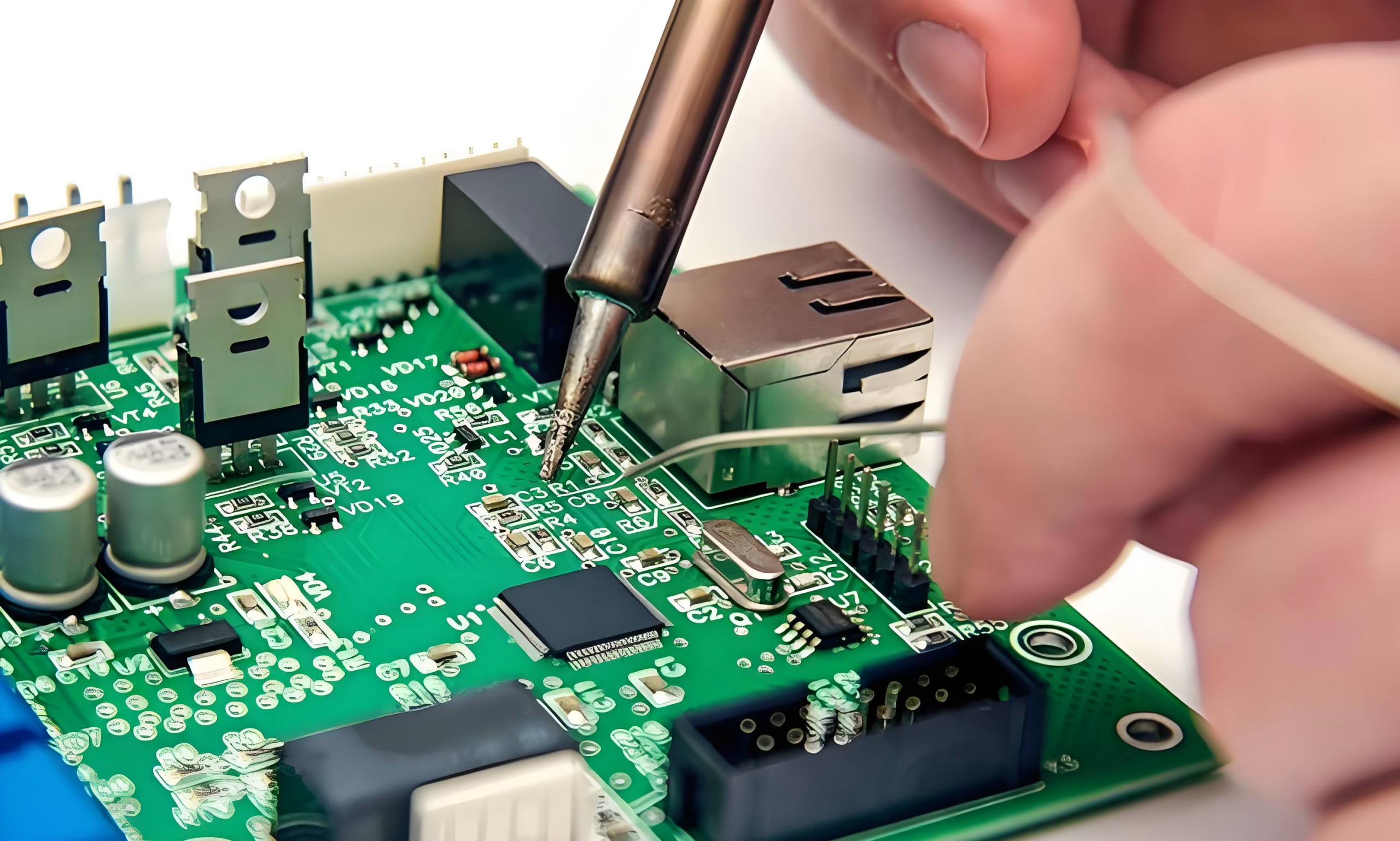
6. How to Rework Circuit Boards with Solder Bridge Issues?
Solder bridges are a common issue during PCB assembly, primarily occurring when solder accidentally connects adjacent pads or pins, causing short circuits. Below are the key rework steps:
1) Locate the Problem
Use a magnifying glass or microscope to identify the solder bridge location. Check if the short is caused by excess solder, component misalignment, or design flaws.
2) Tool Preparation
Constant-temperature soldering iron (300-320°C) or heat gun (with 2mm nozzle);
Desoldering braid/tape, flux, anti-static workstation.
3) Procedure
Remove Excess Solder: Cover the solder bridge area with desoldering braid, heat until solder melts, then absorb it.
Repair Circuitry: For severe solder bridge, use a fine-tip soldering iron to locally etch or cut traces (insulation required).
Clean and Inspect: Clean pads with alcohol and verify no residual shorts under a microscope.
4) Precautions
Control heating time to prevent pad detachment (especially in lead-free processes).
Test circuit continuity post-repair to ensure no latent shorts.
7. Solder Bridge FAQs
A solder bridge is a connection of two or more pads by an excessive application of solder that creates a “bridge” between them.
Solder bridges can be caused by a lot of things, ranging from bad solder paste stencils or bad placement registration to messy assembly lines or clumsy rework techs.
Add solder mask between the pads.
Design the pads and stencil aperture to the right size.
Do not mix old and new flux together.
Adjust the solder paste printing pressure.
Adjust the pressure for pick and place nozzles.
Ensure there is a zero print gap between the PCB and the stencil.
Visual Inspection: Use a magnifying glass or microscope to check for visible solder connections between adjacent pads or pins. Bridges often appear as small blobs or lines of solder where there should be separation.
Electrical Testing: If your circuit isn’t working as expected, use a multimeter set to continuity mode.
Flux can help remove oxides, enhance the wetting properties of the solder, thereby improving the quality of welding. Improve the activity of the flux can reduce the possibility of bridging, because the flux can better wet the pad, so that the welding more uniform.
The primary cause is an excess of solder paste being deposited or paste flowing where it shouldn’t.
8. Summary
PCB assembly solder bridge issues are “invisible killer” in electronics manufacturing. Only by understanding their causes, hazards, and identification methods can it be effectively avoided during production and maintenance, ensuring stable operation of electronic devices. In fact, achieving precise control at every step may not always be feasible in actual production. However, selecting a reliable, experienced PCB assembly partner capable of maintaining quality control is essential. Armed with knowledge on preventing solder bridge issues, you can focus on evaluating PCBA assembly factories’ processes and reflow profiles during vetting. This approach helps minimize uncontrollable costs stemming from bridging-related issues.
Table of Contents

Get Your PCB Quote!