PCB Impedance Control: What It Is and How to Calculate?
PCB impedance is the ratio of voltage to current in a high-speed signal. To ensure signal integrity and prevent data errors, designers must precisely calculate trace width, dielectric height, and constant.
Get Your PCB Quote!
Table of Contents
- 1. Што такое характарыстычны імпеданс у друкаваных платах?
- 2. Чаму кантроль імпедансу мае вырашальнае значэнне для цэласнасці сігналу
- 3. Ключавыя фактары, якія ўплываюць на імпеданс друкаванай платы
- 4. Разлік імпедансу
- 5. Наступствы некантраляванага імпедансу
- 6. Найлепшыя практыкі рэалізацыі кантролю імпедансу
- 7. FAQ
- 8. Рэзюмэ
From blazing-fast processors to high-bandwidth data transmission, modern electronic devices rely on signals traveling across printed circuit boards (PCBs) at incredible speeds. But as signal frequencies soar into the megahertz and gigahertz range, a critical phenomenon known as “impedance” becomes paramount. Uncontrolled impedance can wreak havoc on signal integrity, leading to data errors, system malfunctions, and even complete failure. This is where impedance control steps in, transforming a mere electrical pathway into a precisely engineered transmission line.
1. What is Characteristic Impedance in PCBs?
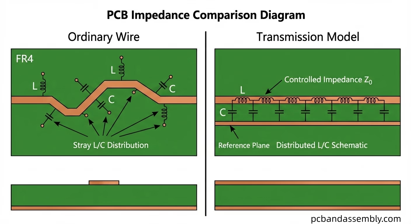
At its core, characteristic impedance (Z₀) of a transmission line, such as a trace on a PCB, is the ratio of the voltage to the current of a single wave propagating down the line, assuming an infinitely long line and no reflections. Unlike simple DC resistance, impedance is a dynamic property that becomes significant when the signal wavelength becomes comparable to or shorter than the length of the trace. This typically occurs at frequencies above 50 MHz, though the exact threshold depends on the trace length and signal rise time.
Think of it like this: when a high-frequency signal travels along a PCB trace, the trace itself starts to behave less like a simple wire and more like a waveguide. It has capacitance between the trace and its reference plane (ground or power plane ) and inductance along its length. These distributed capacitance and inductance combine to define its characteristic impedance. Common target impedance values in PCB design are 50 Ohms for single-ended signals and 100 Ohms for differential pairs, largely due to historical reasons and practical manufacturing considerations, though specific applications may dictate different values.
2. Why Impedance Control is Critical for Signal Integrity
The primary reason for implementing impedance control is to maintain signal integrity. When a high-speed signal encounters a change in impedance along its path, a portion of the signal energy is reflected back towards the source, much like an echo. These reflections can interfere with the original signal, leading to several detrimental effects:
- Signal Degradation:Reflections distort the signal waveform, making it harder for the receiving component to correctly interpret the data. This can manifest as ringing, overshoot, undershoot, or even false triggering.
- Increased Jitter:Variations in signal timing (jitter) can occur due to reflections, impacting the synchronization between components and potentially leading to data errors in high-speed serial links (e.g., PCIe, USB 3.0, Ethernet).
- Crosstalk:Reflections can couple onto adjacent traces, causing unwanted noise and interference, known as crosstalk.
- Electromagnetic Interference (EMI):Poorly controlled impedance can lead to signals radiating energy, contributing to EMI that can affect other circuits or even external devices.
- Reduced System Performance:Ultimately, these issues can lead to reduced clock speeds, increased bit error rates (BER), and overall system instability.
By carefully controlling the impedance of PCB traces, designers ensure that signals propagate smoothly from source to load with minimal reflections, preserving their waveform integrity and ensuring reliable system operation, especially for applications involving high-speed signals measured in GHz.
3. Key Factors Influencing PCB Impedance
Several interdependent factors dictate the characteristic impedance of a PCB trace. Understanding these elements is crucial for accurate impedance calculation and effective design.
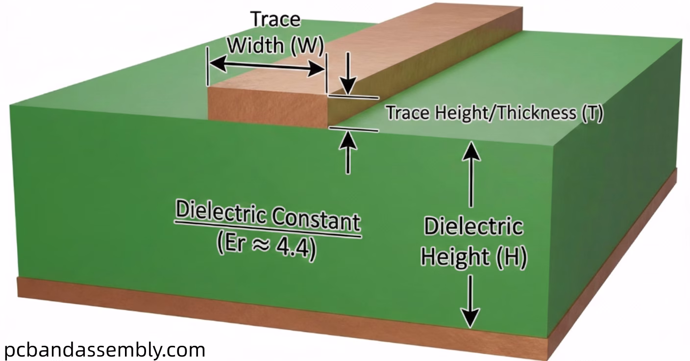
3.1. Trace Geometry
- Trace Width (W):Wider traces generally have lower impedance because they offer more surface area for current flow and higher capacitance to the reference plane. Conversely, narrower traces have higher impedance.
- Trace Height/Thickness (T):Thicker traces (copper weight) also tend to slightly lower impedance by increasing the cross -sectional area, though its effect is less pronounced than width.
3.2. Dielectric Material
- Dielectric Constant (Er or Dk):This is one of the most significant factors. The dielectric constant represents the insulating material’s ability to store electrical energy. A higher dielectric constant (e.g., FR-4’s Dk is around 4.2-4.7) leads to higher capacitance between the trace and its reference plane, thus lowering impedance. Materials with lower Dk (e.g., some specialty laminates like Rogers have Dk around 3) result in higher impedance for the same geometry.
- Dielectric Height (H):This is the thickness of the insulating layer between the trace and its reference plane. A smaller dielectric height results in higher capacitance and thus lower impedance. Conversely, a larger height results in lower capacitance and higher impedance.
3.3. Reference Planes
A continuous, unbroken ground plane or power plane beneath or above a signal trace provides a clear return path for the signal current. The presence and proximity of these planes are fundamental to defining the trace’s characteristic impedance. A trace without a proper reference plane behaves unpredictably.
3.4. Stackup Configuration
The PCB stackup defines the arrangement of copper layers and dielectric layers. It determines whether a trace is a microstrip (on an outer layer) or a stripline (embedded between two reference planes), each having different impedance characteristics. The specific arrangement of dielectric layers and their thicknesses directly impacts the dielectric height (H) and thus the impedance.
4. Calculating Impedance
While exact impedance calculation often involves complex electromagnetic field solvers, simplified analytical formulas provide a good starting point for common trace geometries. These formulas are derived from transmission line theory and consider the factors mentioned above. Manufacturers and design software typically use these more sophisticated models for precision.
4.1. Single-Ended Impedance
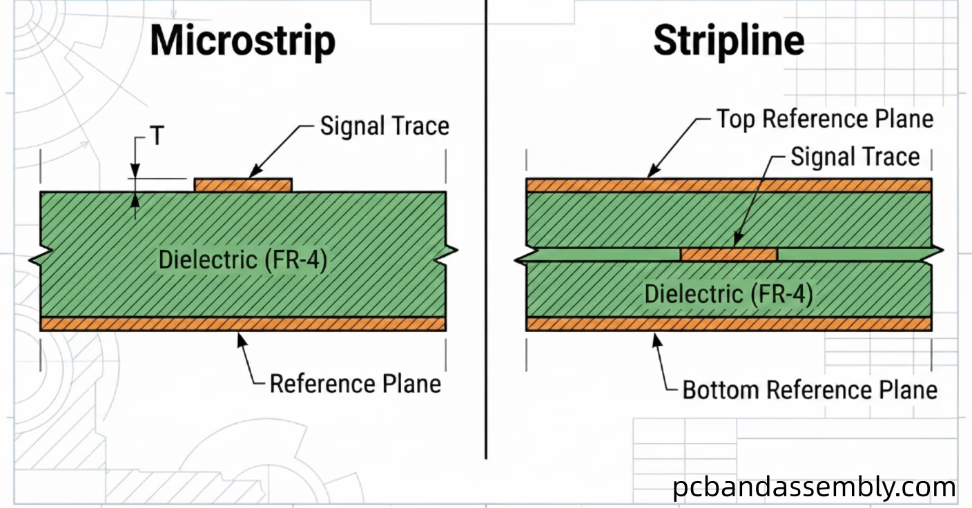
Single-ended traces refer to a single signal line with a reference to a ground or power plane. The two most common configurations are microstrip and stripline.
4.1.1. Microstrip Configuration
A microstrip trace is located on an outer layer of the PCB, separated from a single reference plane by a dielectric layer. It’s often easier to route and inspect but is more susceptible to EMI radiation and external noise.
| Parameter | Description |
| W | Trace width |
| T | Trace thickness (copper weight) |
| H | Height of dielectric between trace and reference plane |
| Er | Dielectric constant of the PCB material |
Example Formula (Simplified for conceptual understanding, actual formulas are more complex):
![]()
4.1.2. Stripline Configuration
A stripline trace is embedded within the inner layers of the PCB, sandwiched between two reference planes (usually ground planes). This configuration offers better signal integrity, shielding, and reduced EMI/crosstalk, but requires more complex stackup design.
| Parameter | Description |
| W | Trace width |
| T | Trace thickness (copper weight) |
| H1 | Height of dielectric between trace and upper reference plane |
| H2 | Height of dielectric between trace and lower reference plane |
| Er | Dielectric constant of the PCB material |
Example Formula (Simplified): ![]() where
where ![]() (total dielectric height)
(total dielectric height)
4.2. Differential Impedance
Differential impedance refers to the impedance between two closely coupled traces that carry complementary signals (one positive, one negative). This configuration is widely used for high-speed serial interfaces because of its excellent noise rejection and reduced EMI. The coupled traces also have an odd-mode and even-mode impedance , but typically, we are concerned with the differential impedance (), which is twice the odd-mode impedance.
4.2.1. Coupled Microstrip
Two traces on an outer layer , separated from a single reference plane by a dielectric layer, and also separated from each other by a small gap (S).
| Parameter | Description |
| W | Individual trace width |
| S | Spacing between traces |
| T | Trace thickness |
| H | Height of dielectric between traces and reference plane |
| Er | Dielectric constant of the PCB material |
Formulas for differential impedance are much more complex, often requiring numerical methods.
4.2.2. Coupled Stripline
Two traces embedded between two reference planes, coupled together with a small gap (S).
| Parameter | Description |
| W | Individual trace width |
| S | Spacing between traces |
| T | Trace thickness |
| H1 | Height of dielectric between traces and upper reference plane |
| H2 | Height of dielectric between traces and lower reference plane |
| Er | Dielectric constant of the PCB material |
Again, precise calculation for differential striplines heavily relies on field solvers.
4 .3. Tools for Calculation
Instead of manual calculations, PCB designers widely use specialized tools for impedance control:
- Impedance Calculators:Many PCB manufacturers provide online calculators based on their specific materials and processes.
- EDA Software:Advanced PCB design suites (e.g., Altium Designer, Cadence Allegro, Eagle) include built-in impedance calculators that integrate with the layer stackup editor.
- Field Solvers:Dedicated electromagnetic field solver software provides the most accurate results by simulating the electromagnetic fields around the traces.
To ensure your design meets signal integrity requirements, you can use our [PCB impedance calculator] for quick calculations; simply enter the parameters and get the results with a single click.

5. The Consequences of Uncontrolled Impedance
Failing to implement proper impedance control can lead to a cascade of problems, directly impacting product reliability and performance.
- Excessive Signal Reflections:The most immediate consequence. A mismatch between the source, transmission line, and load impedance causes signal energy to reflect, creating standing waves and distorting the original signal. This can lead to false triggering of logic gates or missed data bits.
- Increased Crosstalk:Mismatched impedance can exacerbate inductive and capacitive coupling between adjacent traces, leading to signals on one trace interfering with signals on another. This is particularly problematic for dense designs with parallel traces.
- Higher EMI/EMC Issues:Reflections and uncontrolled signal currents can act as miniature antennas, radiating electromagnetic energy. This can cause the product to fail Electro-Magnetic Compatibility (EMC) compliance testing and interfere with other electronic systems.
- Data Corruption and Timing Errors:Distorted signals and reflections can lead to an increase in bit error rates (BER) in digital communication, making it impossible to transmit data reliably. For sensitive analog signals, this translates to noise and inaccuracy.
- Reduced Operational Speed:To compensate for poor signal integrity, designers might be forced to reduce clock frequencies, hindering the device’s potential performance.
- System Instability and Failures:In severe cases, uncontrolled impedance can lead to intermittent system crashes, unexplained behavior, or complete device malfunction, making debugging a nightmare.
6. Best Practices for Implementing Impedance Control
Achieving successful impedance control requires a holistic approach throughout the PCB design and manufacturing process.
- Collabor ate with Manufacturers Early:Share your target impedance values and stackup requirements with your PCB fabricator early in the design cycle. They can advise on achievable trace geometries and material options for their specific processes.
- Careful Material Selection:Choose PCB laminates with consistent and well-defined dielectric constants (Er) that meet your signal integrity requirements. For very high-speed applications (e.g., RF, mmWave), specialized low-loss materials are essential .
- Optimized Stackup Design:Design a stackup that provides continuous reference planes for all signal layers. Ensure consistent dielectric heights (H) for controlled impedance traces. Burying high-speed traces (stripline ) offers better shielding.
- Consistent Trace Geometry:Maintain uniform trace widths and spacing (for differential pairs) along the entire length of the controlled impedance route. Avoid abrupt changes in width, sharp corners, and unnecessary vias where possible, as these introduce impedance discontinuities.
- Dedicated Reference Planes:Ensure that controlled impedance traces have a solid, uninterrupted ground or power plane directly beneath (or above) them to provide a clean return path. Avoid splitting reference planes under high-speed signals.
- Minimizing Discontinuities:Vias, pads, and component footprints can create impedance discontinuities. Minimize the number of vias in critical traces and optimize pad designs. Back drilling vias can help reduce stub reflections in very high-speed designs.
- Precise Manufacturing Tolerances:Specify tight tolerances for trace width, copper thickness, and dielectric height to the manufacturer. Understand that even with control , there will be variations, and design to accommodate them.
- Testing and Validation:After manufacturing, use a Time Domain Reflectometer (TDR) to measure the actual characteristic impedance of critical traces. This helps validate the design and manufacturing process.
7. FAQ
Question1:What is the most common impedance target for single-ended signals?
Answer: 50 Ohms is the most common target impedance for single-ended signals in many digital and RF applications, mainly due to a balance of practical manufacturing limits and component compatibility.
Question2:What is the most common impedance target for differential signals ?
Answer: 100 Ohms is the standard target differential impedance for many high-speed serial interfaces like USB, PCIe, and Ethernet.
Question3:What happens if my trace impedance is too high or too low?
Answer: If trace impedance is too high or too low compared to the source/load impedance, signal reflections will occur. This can lead to signal distortion, increased jitter, crosstalk, and EMI, ultimately causing data errors and system instability.
Question4:Can I control impedance without a ground plane?
Answer: No, a continuous reference plane (typically a ground plane, but sometimes a power plane) is essential for defining the characteristic impedance of a trace and providing a proper return path for high-frequency signals. Without it, the impedance is undefined and uncontrolled.
Question5:How does PCB stackup affect impedance control?
Answer: The stackup critically determines whether a trace is microstrip or stripline, the dielectric height (H), and the proximity to reference planes. All these factors directly influence the trace’s characteristic impedance. A well-designed stackup is fundamental to achieving controlled impedance.

8. Summary
By precisely defining the characteristic impedance of signal traces, designers mitigate signal reflections, minimize crosstalk, reduce EMI, and ensure robust signal integrity. This is achieved through careful consideration of trace geometry, dielectric material properties, and the PCB stackup configuration. While complex calculations are involved, advanced EDA tools and collaboration with experienced manufacturers empower engineers to meet stringent impedance targets.
Table of Contents
- 1. Што такое характарыстычны імпеданс у друкаваных платах?
- 2. Чаму кантроль імпедансу мае вырашальнае значэнне для цэласнасці сігналу
- 3. Ключавыя фактары, якія ўплываюць на імпеданс друкаванай платы
- 4. Разлік імпедансу
- 5. Наступствы некантраляванага імпедансу
- 6. Найлепшыя практыкі рэалізацыі кантролю імпедансу
- 7. FAQ
- 8. Рэзюмэ

Get Your PCB Quote!