PCB Layers Explained: Everything You Need to Know
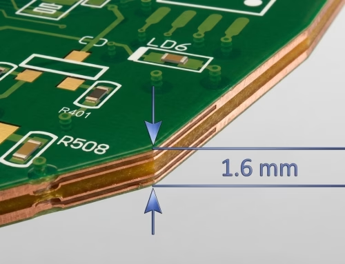
A PCB is a "sandwich" structure formed by alternating layers of conductive material—typically copper foil—and insulating materials such as FR-4 substrates, Core, and Prepreg. Furthermore, it includes a solder mask to protect the circuitry and a silkscreen layer to provide essential identification information.
Get Your PCB Quote!

1. Introduction
Printed Circuit Boards (PCBs) are the unsung heroes powering virtually every electronic device in our lives, from smartphones and smart appliances to complex industrial machinery. Often referred to as the “back bone” of modern electronics, PCBs provide the mechanical support and electrical connections for electronic components.
While the concept of a circuit board might seem straightforward, the intricacy often lies beneath the surface – quite literally – in its layers. Just as a building requires multiple floors to maximize space and functionality, a PCB utilizes a stack of conductive and insulating layers to achieve its complex tasks. Understanding these PCB layers is crucial for anyone looking to grasp how electronic devices are designed and manufactured, influencing everything from signal speed to power distribution and overall device performance.
2. What Are PCB Layers?
At its core, a Printed Circuit Board is a laminated sandwich structure made up of alternating conductive and insulating layers. Each “PCB layer” is essentially a thin sheet of material that plays a specific role in the board’s functionality. The conductive layers, typically made of copper, feature patterns of traces, pads, and planes that act like wires, guiding electrical signals and power across the board. These are interspersed with insulating layers that prevent electrical short circuits between the conductive parts, maintaining signal integrity and power distribution.
Historically, early PCBs used only one or two copper layers. However, advancements in manufacturing technology have enabled the creation of complex multi-layer PCBs, allowing for more compact designs, enhanced functionality, and improved performance in modern electronic devices. The ability to stack multiple conductive layers interconnected by tiny, metal-lined drilled holes called vias is what truly revolutionized circuit board design.
3. Essential Components of a PCB Layer
Regardless of the number of layers, all PCBs are constructed from a few fundamental materials, each serving a critical purpose:
- Substrate (Core):This is the foundational non-conductive, insulating material, typically made from fiberglass-reinforced epoxy resin (FR-4). The core is a cured, solid laminate that provides mechanical strength and electrical insulation. Traces are often placed directly on or within core layers.
- Copper Foil:These are the conductive layers where the circuit design is etched. Copper foil is laminated onto or between the substrate layers. After etching, the remaining copper forms the traces, pads, and planes that carry electrical signals and power.
- Prepreg:Short for “pre-impregnated,” prepreg is a thin sheet of fiberglass impregnated with an uncured epoxy resin. It acts as an adhesive to bind the copper foil and core layers together during the lamination process. When heated and pressed, the resin in the prepreg cures, forming a solid, insulating bond.
- Solder Mask :This is a protective, non-conductive layer, typically green (though other colors exist), applied over the copper traces on the outer surfaces of the PCB. Its primary function is to prevent solder bridges (unwanted electrical connections) between adjacent pads or traces during component assembly and to protect the copper from oxidation and environmental contaminants.
- Silkscreen:Applied on top of the solder mask, the silkscreen layer provides visible alphanumeric characters, symbols, and outlines. This layer is crucial for indicating component positions, polarity, test points, and other helpful markings for assembly, testing, and troubleshooting.
4 . Types of PCBs by Layer Count
PCBs are categorized based on the number of conductive copper layers they contain. This classification directly impacts their complexity, manufacturing cost, and suitability for various applications.
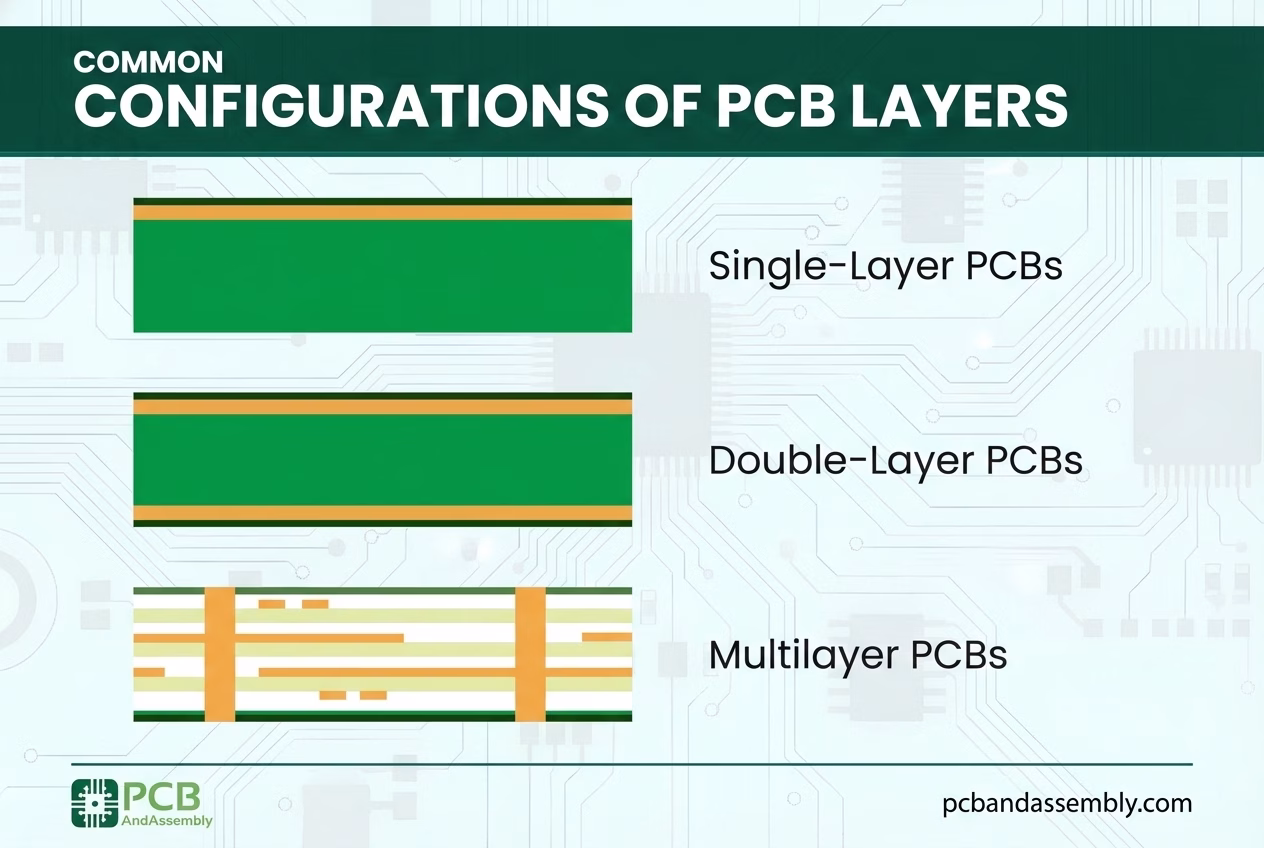
4.1. Single-Layer PCBs
As the name suggests, a single-layer PCB (or single-sided PCB) features just one layer of conductive copper traces on a non- conductive insulating substrate. Components are typically mounted on one side, and the copper traces are on the opposite side. They are the simplest and most cost-effective PCBs to manufacture, making them ideal for less complex electronic devices.
- Structure:Consists of a substrate, one copper layer, a solder mask, and a silkscreen layer.
- Applications:Simple electronics like calculators, LED lighting, basic toys, and power supplies.
- Advantages:Low cost, easy to design and troubleshoot, quick manufacturing.
- Disadvantages:Limited circuit density, can’t handle complex designs, larger footprint for a given circuit.
4.2. Double-Layer PCBs
Also known as double-sided PCBs, these boards have two conductive copper layers – one on the top surface and one on the bottom surface of the insulating substrate. Electrical connections between the top and bottom layers are made using vias. This allows for significantly increased circuit density and flexibility compared to single-layer boards.
- Structure :Substrate sandwiched between two copper layers, with solder mask and silkscreen on both outer sides. Vias connect the layers.
- Applications:USB systems, power amplifiers, vending machines, simple medical devices, and many consumer electronics.
- Advantages:Higher circuit density, more flexible routing, reduced size compared to single-layer for same circuit.
- Disadvantages:More complex to design and manufacture than single-layer, higher cost.
4.3. Multi-Layer PCBs
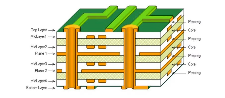
Multilayer PCBs incorporate three or more conductive copper layers, separated by insulating layers of core and prepreg, and laminated together under high temperature and pressure. These boards can range from 4 layers to 60+ layers, enabling incredibly dense and complex circuit designs. The internal layers are often dedicated to specific functions, such as signal routing , ground planes, and power planes.
- Structure:Multiple core and prepreg layers stacked with copper foil in between, all laminated together. Vias (through-hole, blind, or buried) connect specific layers.
- Applications:High-performance electronics such as computers, servers, smartphones, GPS technology, medical equipment, and aerospace systems.
- Advantages:Extremely high circuit density, smaller form factor, improved signal integrity, better EMI shielding, enhanced power distribution.
- Disadvantages:High manufacturing cost, complex design and fabrication, difficult to repair.
Here’s a quick comparison of PCB types :
| Feature | Single-Layer PCB | Double-Layer PCB | Multi-Layer PCB |
| Copper Layers | 1 | 2 | 3+ (commonly 4, 6, 8, 10, etc.) |
| Complexity | Low | Medium | High |
| Cost | Low | Medium | High |
| Circuit Density | Low | Medium | Very High |
| Signal Integrity | Basic | Improved | Excellent |
| Size Potential | Larger | Smaller | Smallest for complex circuits |
| Applications | Calculators, simple sensors | USB, LED lighting | Smartphones, computers, servers |
5. Internal Layers of Multilayer PCBs
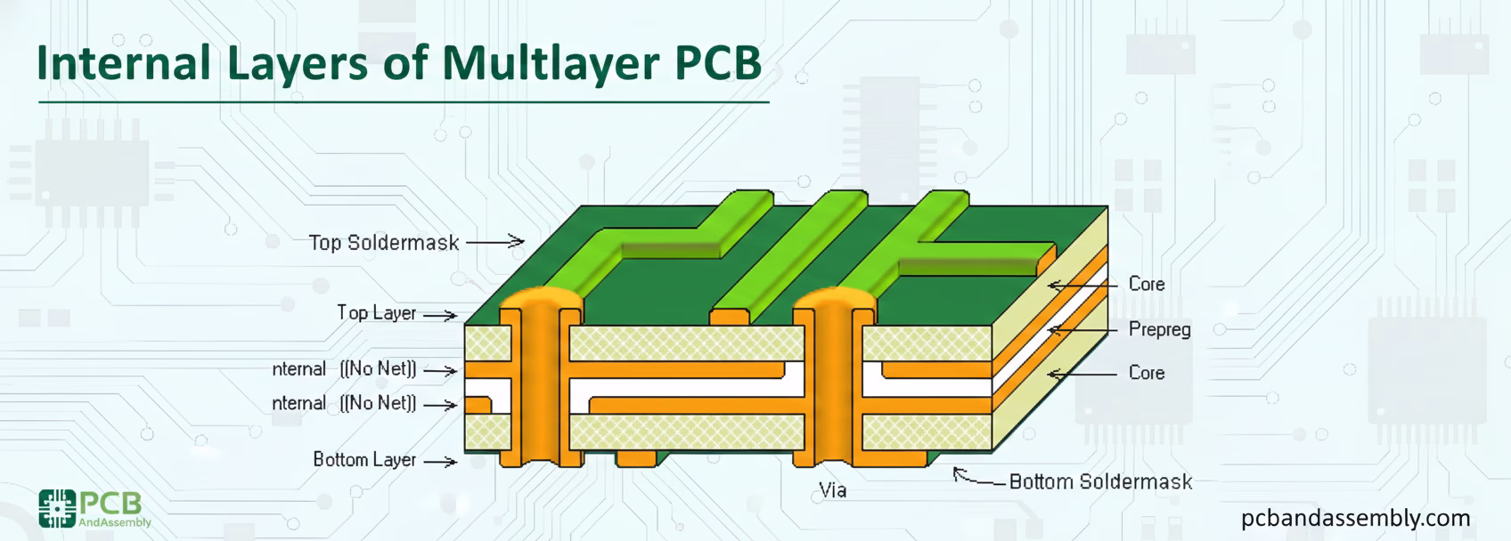
The true power of a multilayer PCB lies in the strategic arrangement and purpose of its internal layers. These layers are not just for routing signals but also play a critical role in managing power and ground distribution, which significantly impacts the board’s overall performance and reliability.
5.1. Signal Layers
These layers are primarily dedicated to routing the conductive traces that carry data and control signals between electronic components. In multilayer boards, multiple signal layers allow for highly intricate and dense routing, crucial for complex circuits found in modern high-speed digital devices. By distributing signals across several layers, designers can minimize crosstalk and reduce electromagnetic interference (EMI).
5.2. Ground Planes
A ground plane is a large, continuous area of copper on an internal layer that serves as the common return path for current from various components. It provides a stable zero-volt reference, helping to reduce noise and improve signal integrity. A well-designed ground plane also acts as a shield against EMI and aids in heat dissipation.
5.3. Power Planes
Similar to ground planes, power planes are large copper areas dedicated to distributing specific supply voltages across the board ( e.g., +3.3V, +5V). Having dedicated power planes ensures a stable and low-impedance power supply to components, crucial for consistent performance, especially in high-current or high-speed applications. They also help in filtering noise from the power supply.
6. The Importance of PCB Layer Stackup
The “PCB layer stackup” refers to the specific order and arrangement of conductive and insulating layers within a multilayer board. This isn’t just a random stacking; it’s a meticulously planned design element that profoundly impacts the PCB’s electrical performance, manufact urability, and cost.
A well-optimized layer stackup is crucial for:
- Signal Integrity:Proper stackup helps control impedance, minimize signal reflections, and reduce crosstalk between adjacent traces, ensuring signals arrive at their destination accurately.
- Electromagnetic Compatibility (EMC):By strategically placing ground planes next to signal layers, designers can create effective shielding against electromagnetic interference (EMI), both emitted by the board and absorbed from external sources.
- Power Distribution:Dedicated power and ground planes provide stable voltage and current delivery, minimizing voltage drops and power supply noise.
- Thermal Management:Copper layers, especially ground and power planes, can help dissipate heat generated by components, contributing to the board’s longevity and reliability.
- Cost and Manufacturability:The number of layers and the materials used directly affect manufacturing complexity and cost. An efficient stackup can achieve desired performance with fewer layers, optimizing cost.
For example, a common 4-layer stackup might be: Signal (Top) / Ground / Power / Signal (Bottom). More complex boards might have alternating signal, ground, and power planes to achieve specific impedance or shielding requirements.
7. Benefits of Mult ilayer PCBs
The evolution from single to multilayer PCBs has brought numerous advantages, particularly as electronic devices become more sophisticated and compact:
- Increased Functionality and Density:Multilayer boards allow for significantly more circuit complexity within a smaller footprint, enabling feature-rich devices without increasing their physical size.
- Reduced Size and Weight:By routing signals vertically through layers instead of horizontally across a large single plane, multilayer PCBs help miniaturize electronic products. This is critical for portable devices.
- Improved Performance:Strategic placement of ground and power planes, along with optimized signal layers, leads to better signal integrity, reduced noise, and more stable power delivery , all contributing to superior electrical performance.
- Enhanced EMI Shielding:Internal ground planes act as effective shields, containing electromagnetic radiation and protecting the circuit from external interference.
- Better Heat Dissipation:The larger copper areas of power and ground planes can help conduct heat away from components, improving the thermal management of the PCB.
- Increased Durability:The laminated structure of multilayer PCBs often results in a more rigid and robust board that can withstand environmental stresses better than thinner, single-layer alternatives.
8. PCB Layers FAQ
1). What is the difference between a core and a prepreg in a PCB?
A core is a rigid, cured laminate, typically fiberglass-reinforced epoxy, that serves as a base with copper foil already bonded to it. Prepreg, on the other hand, is a thin, flexible sheet of fiberglass impregnated with uncured epoxy resin. It acts as an adhesive and insulating layer, bonding core and copper foil layers together during the lamination process.
2). How many layers can a PCB have?
While PCBs typically range from 1 to 16 layers, highly specialized applications can feature PCBs with 40 layers or even more, particularly in advanced computing or military hardware.
3). Why are vias important in multilayer PCBs?
Vias are crucial because they create electrical interconnections between different conductive layers of a multilayer PCB. Without vias, signals and power would be confined to a single layer, making complex, dense routing impossible and negating the advantages of having multiple layers. They allow for vertical connections, dramatically increasing routing flexibility and circuit density.
4). What is the most common material used for PCB insulating layers?
FR-4 (Flame Retardant 4), a fiberglass-epoxy laminate, is the most widely used material due to its good balance of electrical properties, mechanical strength, and cost-effectiveness.
5). Can I design a high-speed circuit on a single-layer PCB?
While technically possible for very simple, low-speed signals, it is generally not recommended for high-speed circuits. Single-layer PCBs lack dedicated ground and power planes, making it difficult to control impedance, manage signal return paths, and mitigate EMI effectively. High-speed signals require careful impedance control and robust ground planes, which are best achieved with multilayer PCB designs.
9. Summary
Printed Circuit Board layers are the fundamental building blocks of virtually all modern electronics. From the simplest single-layer boards to the most complex multilayer designs, each PCB is a meticulously engineered stack of conductive copper and insulating materials. The core components include the substrate (core), copper foil, prepreg, solder mask, and silkscreen, each serving a vital role in providing mechanical support, electrical connectivity, and protection.
As electronic devices demand greater functionality in smaller packages , the evolution towards double-layer and increasingly sophisticated multi-layer PCBs has become essential. Multilayer boards offer benefits such as higher circuit density, improved signal integrity, better power distribution through dedicated ground and power planes, and enhanced EMI shielding. The careful planning of a PCB’s layer stackup is not merely a manufacturing step but a critical design decision that dictates the board’s electrical performance and overall reliability.
Understanding these layers is key to appreciating the intricate engineering behind the devices that power our connected world, ensuring stable, efficient, and high-performance electronics.

Get Your PCB Quote!