What is an 8-Layer PCB Stackup? Performance & Design Secrets
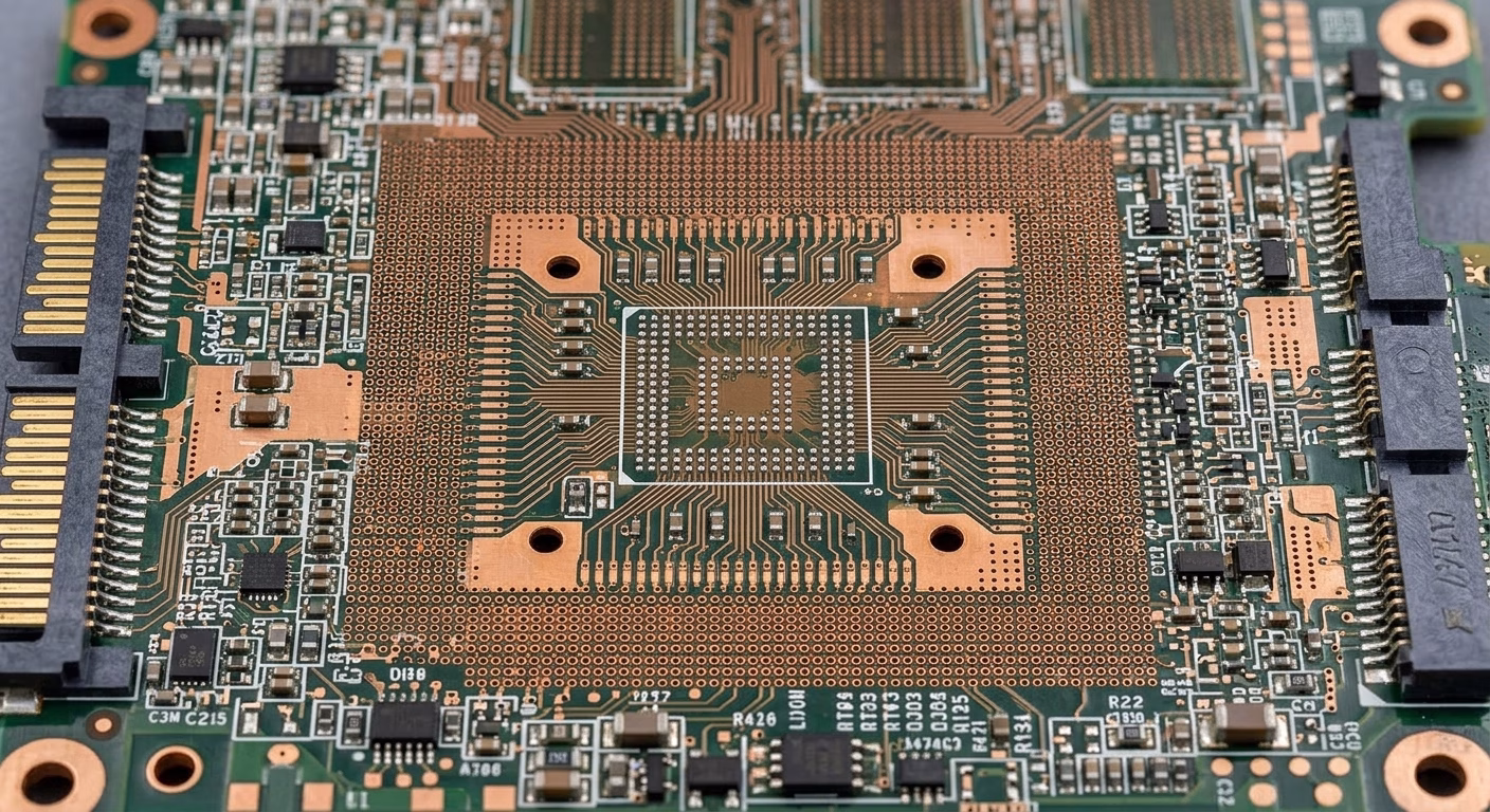
An 8-layer PCB stackup is a printed circuit board composed of eight distinct conductive (copper) layers separated by insulating dielectric layers. At PCBAndAssembly, we specialise in PCB manufacturing, ensuring that your 8-layer stackup meets the highest standards for quality and reliability.
Get Your PCB Quote!
Table of Contents
- 1. परिचय
- 2. 8-लेयर पीसीबी स्टैकअप क्या है?
- 3. 8-लेयर पीसीबी स्टैकअप क्यों चुनें?
- 4. 8-लेयर स्टैकअप के प्रमुख घटक
- 5. सामान्य 8-परत स्टैकअप कॉन्फ़िगरेशन
- कॉन्फ़िगरेशन 3: ग्राउंड–सिग्नल–ग्राउंड–सिग्नल–सिग्नल–पावर–सिग्नल–ग्राउंड
- 6. बोर्ड की मोटाई और परत के आयाम
- 7आवश्यक डिज़ाइन दिशानिर्देश और सर्वोत्तम अभ्यास
- 8. 8-लेयर पीसीबी की निर्माण प्रक्रिया
- 98-लेयर पीसीबी के अनुप्रयोग
- 10. 8-लेयर पीसीबी स्टैकअप की चुनौतियाँ
- 11. सामान्य प्रश्न
- 12। सारांश

1. Introduction
As devices become more compact , complex, and demand higher performance, the humble PCB has had to evolve significantly. While single-layer and two-layer boards suffice for simpler applications, modern electronics frequently require multilayer PCBs to manage intricate circuitry, high-speed signals, and stringent electromagnetic compatibility (EMC) requirements.
Among these sophisticated designs, the 8-layer PCB stackup stands out as a widely adopted configuration. It strikes a crucial balance—offering superior functionality over simpler 4-layer or 6-layer designs without the extreme complexity and cost of higher layer counts. This guide explores the structure, materials, configurations, and critical design guidelines engineers need to harness the full potential of 8-layer PCBs.
2. What is an 8-Layer PCB Stackup?

At its core, an 8-layer PCB stackup is a printed circuit board composed of eight distinct layers of conductive material (copper) separated by insulating dielectric layers. These layers are meticulously stacked and bonded together to form a robust and electrically functional unit. This multilayer PCB design allows for highly complex routing paths within a compact footprint, a necessity for today’s space-constrained devices. Unlike simpler boards, an 8-layer configuration provides ample room to dedicate layers specifically for signal routing, power distribution, and ground planes.
Typically, an 8-layer stackup consists of four signal layers and four plane layers (ground and power planes). The strategic placement of these plane layers is crucial; they act as shields and provide stable reference voltages for the signal layers, effectively distributing power across the board and enhancing overall electrical performance. This arrangement is fundamental to maintaining signal integrity and mitigating issues like noise and crosstalk, which become critical challenges in high-speed digital designs. The flexibility offered by these multiple layers makes 8-layer PCBs ideal for applications demanding high-speed performance without compromising the physical size of the electronic device.
3. Why Choose an 8-Layer PCB Stackup?
The decision to opt for an 8-layer PCB stackup over designs with fewer layers is often driven by a need for enhanced performance , reliability, and design flexibility. Here are the primary reasons why this configuration is a preferred choice for medium to high-complexity electronic designs:
- Superior Signal Integrity:With four dedicated signal layers, designers have greater freedom to route critical high-speed signals with optimal impedance control, minimizing reflections and signal degradation. The presence of multiple ground and power planes provides clear return paths for signals, significantly improving signal quality.
- Enhanced Power Distribution:Dedicated power and ground planes ensure a stable and low-impedance power delivery network across the board. This is vital for components that draw significant current or require very clean power, preventing voltage drops and noise that can affect device operation.
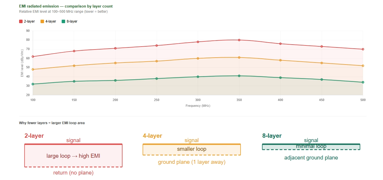
- Reduced Electromagnetic Interference (EMI):The interleaved arrangement of signal and plane layers acts as a natural shield, effectively containing electromagnetic fields and reducing both radiated and conducted EMI. This is crucial for meeting regulatory compliance and ensuring reliable operation in noisy environments.
- Greater Routing Flexibility:More layers mean more routing channels. This allows for more direct and shorter signal paths, which is beneficial for high-speed designs, and makes it easier to manage complex interconnections, especially with high-pin-count components.
- Compactness for Complex Designs:By stacking layers vertically, an 8-layer PCB can accommodate a vast amount of circuitry in a smaller physical area compared to a larger, less layered board. This is indispensable for modern, compact electronic devices.
- Better Thermal Management:Copper planes can also contribute to heat dissipation. A well-designed stackup can leverage these planes to draw heat away from critical components, improving the longevity and reliability of the device.
Compared to 4-layer and 6-layer stackups, an 8-layer board offers a significant leap in managing complex designs, especially those involving advanced consumer electronics, embedded systems, and communication hardware where signal integrity and EMI reduction are paramount. While 10 or 12-layer boards exist, the 8-layer offers an optimal balance between performance and manufacturing cost/ complexity.
4. Key Components of an 8-Layer Stackup
Understanding the fundamental components that make up an 8-layer PCB stackup is crucial for effective design. These boards are constructed from a combination of conductive and insulating materials, meticulously bonded together:
4.1 Copper Layers
Eight copper layers form the conductive network where traces, pads, and planes are etched. Thickness varies based on current-carrying requirements and impedance control needs, with common weights of 0.5 oz/ft² (0.017 mm), 1 oz/ft² (0.035 mm), and 2 oz/ft² (0.070 mm).
Two primary types of copper foil are used:
- Electrodeposited (ED) Copper Foil: Widely used due to excellent conductivity and smooth surface finish, forming reliable conductive pathways across all layers.
- Rolled Annealed (RA) Copper Foil: Preferred for applications requiring mechanical flexibility or bending resistance, providing reliable conduction without compromising structural integrity.
4.2 Core Material
Cores are rigid dielectric sheets with copper laminated on both sides, providing structural backbone and defining fixed distances between adjacent copper layers. Common core materials include:
- FR-4: The industry-standard woven fiberglass/epoxy composite, offering excellent electrical insulation, mechanical strength, EMC performance, and thermal stability across a broad range of applications. Core thickness typically ranges from 0.3–0.5 mm per layer.
- Polyimide: Used in high-performance designs requiring superior temperature resistance or flexible circuits—ideal for extreme environments.
- Rogers Materials: Chosen for high-frequency (RF/microwave) applications due to their low dielectric loss and excellent signal integrity properties.
4.3 Prepreg
Prepreg (pre-impregnated) is fiberglass cloth saturated with partially cured resin. Under heat and pressure during lamination, the resin flows, encapsulates traces, and cures—bonding all layers together. Typical prepreg thickness ranges from 0.1–0.2 mm per sheet. The dielectric constant (Dk) and dissipation factor (Df) of both prepreg and core materials directly influence trace impedance, making material selection critical for high-speed performance.
4.4 Solder Mask
Applied to outer layers to protect copper traces from oxidation and prevent solder bridges during assembly. Two main types:
- Liquid Photoimageable (LPI) Solder Mask: The most common type—precisely applied and UV-cured for high reliability in multilayer PCB protection.
- Dry Film Solder Mask: Used in high-precision applications requiring exceptionally consistent coverage and durability.
4.5 Surface Finish
Surface finishes protect exposed copper pads and ensure solderability. The choice depends on application requirements:
| Surface Finish | Key Characteristics | Best Suited For |
| HASL (Hot Air Solder Leveling) | Reliable solderable surface; low cost; may have uneven surface | General-purpose PCBs with standard component density |
| ENIG (Electroless Nickel Immersion Gold) | Flat surface; excellent corrosion resistance; long shelf life | Fine-pitch components, critical high-reliability applications |
| OSP (Organic Solderability Preservative) | Environmentally friendly; thin organic layer; cost-effective | Consumer electronics with short shelf-life requirements |
4.6 Silkscreen
Epoxy ink silkscreen printing labels components and provides reference information directly on the PCB surface. Its durability and resistance to environmental degradation ensure legibility throughout the board’s operational lifecycle.
5. Common 8-Layer Stackup Configurations
While there’s no single “correct” 8-layer stackup, several common configurations are adopted based on the primary design objectives, such as optimizing signal integrity, minimizing EMI, or simplifying routing. The most common standard layer buildup typically involves an alternating pattern of signal and plane layers.
Here are two widely used 8-layer PCB stackup configurations:
Configuration 1: Signal-Ground-Signal-Power-Power-Signal-Ground-Signal
This configuration prioritizes strong ground and power planes to act as shields and provide stable references for the inner signal layers. The symmetry can also help with thermal expansion.
| Layer Number | Type | Function/Benefit |
| Layer 1 | Signal | Top routing layer, components placed here. |
| Layer 2 | Ground | Primary ground plane, shielding for Layer 1. |
| Layer 3 | Signal | Inner high-speed signal routing. |
| Layer 4 | Power | Dedicated power plane (e.g., VCC), provides reference for Layer 3. |
| Layer 5 | Power | Dedicated power plane (e.g., VDD or another voltage), provides reference for Layer 6. |
| Layer 6 | Signal | Inner high-speed signal routing. |
| Layer 7 | Ground | Secondary ground plane, shielding for Layer 8. |
| Layer 8 | Signal | Bottom routing layer, often for less critical signals or components. |
In this setup , each signal layer (L1, L3, L6, L8) is adjacent to a plane layer (ground or power), which is excellent for impedance control and providing a clear return path for signals, thereby enhancing signal integrity and reducing EMI.
Configuration 2: Ground-Signal-Power-Signal-Signal-Power-Signal-Ground
This configuration places ground planes on the outermost layers, offering maximum shielding from external noise and providing robust return paths for signals from both top and bottom layers. This can be particularly effective for designs sensitive to external EMI.
| Layer Number | Type | Function/Benefit |
| Layer 1 | Ground | Outer ground plane, provides strong EMI shielding and reference for Layer 2. |
| Layer 2 | Signal | Top signal routing layer, components placed here. |
| Layer 3 | Power | Dedicated power plane, provides reference for Layer 2 and Layer 4. |
| Layer 4 | Signal | Inner high-speed signal routing. |
| Layer 5 | Signal | Inner high-speed signal routing (another set of complex routing). |
| Layer 6 | Power | Dedicated power plane, provides reference for Layer 5 and Layer 7. |
| Layer 7 | Signal | Bottom signal routing layer, often for less critical signals. |
| Layer 8 | Ground | Outer ground plane, robust EMI shielding and reference for Layer 7. |
Configuration 3: Ground–Signal–Ground–Signal–Signal–Power–Signal–Ground
This configuration wraps all routing layers within ground planes, including an additional internal ground layer. All signal paths are fully enclosed between ground references, creating highly predictable return current paths and minimizing crosstalk—ideal for densely routed, noise-sensitive designs.
| Layer | Type | Function & Benefit |
| Layer 1 | Ground | Top outer ground; maximum external shielding |
| Layer 2 | Signal | High-speed routing, shielded on both sides by ground |
| Layer 3 | Ground | Internal ground for extra isolation between upper signal layers |
| Layer 4 | Signal | Inner routing with dual ground references |
| Layer 5 | Signal | Inner routing; power plane provides reference below |
| Layer 6 | Power | Centralized power distribution |
| Layer 7 | Signal | Bottom inner routing with power reference above |
| Layer 8 | Ground | Bottom outer ground; strong shielding and return path |
The choice between configurations depends on the specific requirements of the design, including signal speed, noise sensitivity, and power delivery needs. Regardless of the exact arrangement, the principle of providing adjacent ground or power planes for signal layers remains a cornerstone of effective 8-layer PCB design.
6. Board Thickness and Layer Dimensions
The total board thickness of an 8-layer PCB stackup typically falls between 1.57 mm and 2.44 mm (0.062″–0.096″), though the standard 1.6 mm remains the most common. Several factors influence the final thickness:
- Prepreg thickness: 0.1–0.2 mm per sheet, depending on material and resin content
- Core thickness: 0.3–0.5 mm per layer, providing the primary structural contribution
- Copper foil weight: 0.5 oz/ft² (0.017 mm), 1 oz/ft² (0.035 mm), or 2 oz/ft² (0.070 mm)
Thicker copper increases current capacity and heat dissipation but raises impedance calculation complexity. Always consult your PCB manufacturer for their specific tolerance capabilities, as even small deviations in dielectric thickness can shift trace impedance outside acceptable limits.
7. Essential Design Guidelines and Best Practices
Designing an effective 8-layer PCB stackup goes beyond merely stacking layers; it requires adherence to critical guidelines to ensure optimal performance, reliability, and manufacturability.
7.1. Signal Integrity Management
- Impedance Control:For high-speed signals, maintaining consistent characteristic impedance is paramount. This involves carefully selecting dielectric materials (prepreg and core thickness, dielectric constant) and trace width/spacing. Work closely with your PCB manufacturer to ensure their manufacturing capabilities can meet your specified impedance targets.
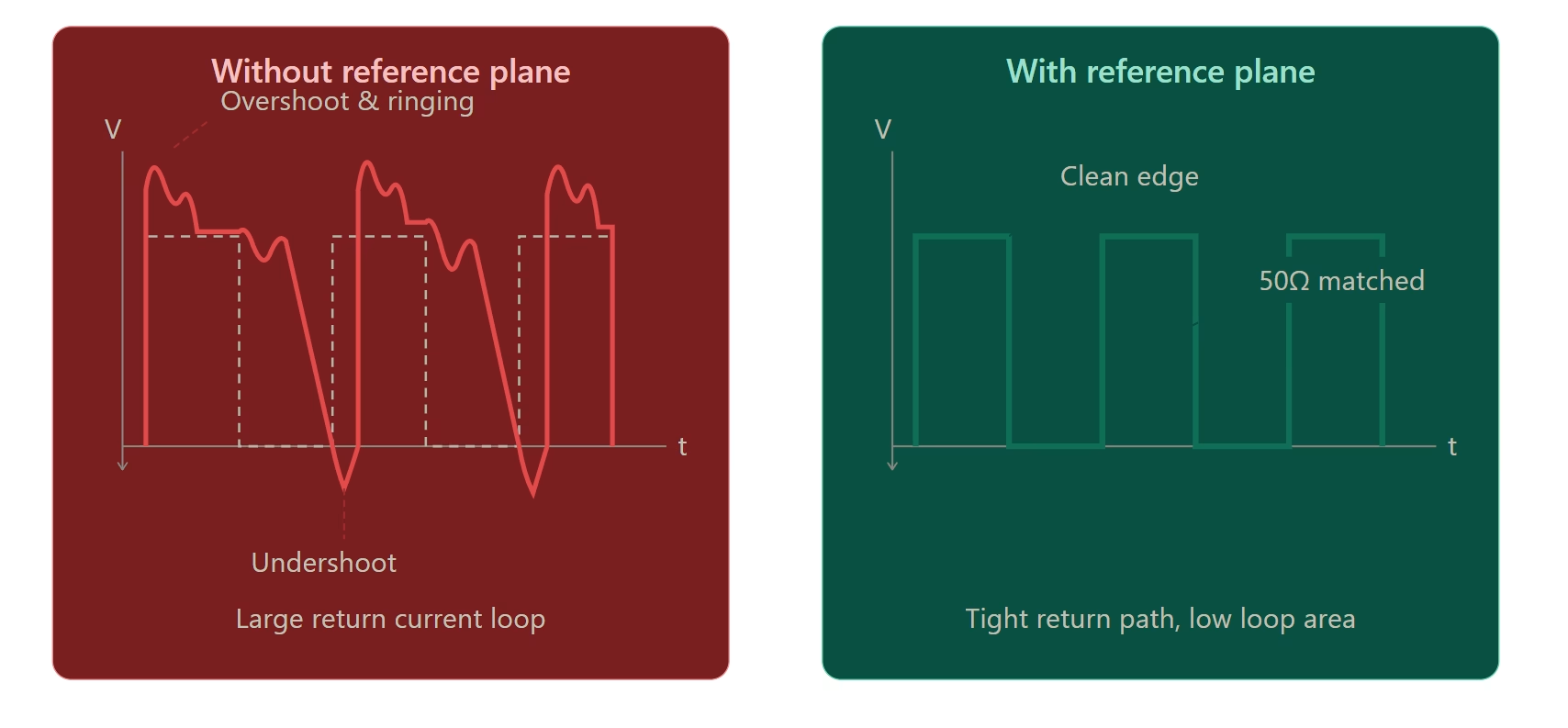
- Clear Return Paths:Ensure every signal trace has an uninterrupted, adjacent ground or power plane acting as a return path. Interruptions ( like splits in planes or crossing gaps) can create unwanted loops, leading to EMI and signal degradation.
- Minimize Stubs:Avoid long stubs on signal traces, especially for high-speed signals, as they can cause reflections. Use vias judiciously.
7.2. Power Distribution Network (PDN) Optimization
- Dedicated Power/Ground Planes:Utilize full, unbroken ground and power planes as much as possible. These planes offer low impedance power delivery and excellent noise suppression.
- Decoupling Capacitors:Place decoupling capacitors close to the power pins of ICs, connecting them directly to the power and ground planes with short, wide traces to minimize inductance. This helps filter noise and provide transient current.
- Minimize Plane Splits:Avoid splitting power or ground planes unless absolutely necessary, and if so, understand the implications for signal return paths. Splits can severely degrade performance by forcing return currents to take longer, inductive paths.
7.3. Electromagnetic Interference (EMI) Reduction
- Stackup Symmetry:Aim for a balanced stackup to prevent warping during manufacturing and improve EMI performance. Symmetric placement of dielectric materials and copper weights can help.
- Shielding:Ground planes provide excellent shielding. Ensure critical high-speed signal layers are sandwiched between ground planes whenever possible to maximize EMI containment.
- Controlled Current Loops:Keep high-frequency current loops as small as possible by ensuring tight coupling between signal traces and their return planes.
7.4. Material Selection and Thickness
- Dielectric Properties:Choose prepreg and core materials with appropriate dielectric constants (Dk) and dissipation factors (Df) for your operating frequencies. Lower Dk values are generally preferred for high-speed applications .
- Overall Board Thickness:The total board thickness, combined with individual layer thicknesses, influences impedance and mechanical strength. Standard thicknesses like 1.6mm (62 mils) are common, but specific application needs might dictate variations.
7.5. Manufacturing Considerations (DFM)
- Consult Your Manufacturer:Engage with your chosen PCB manufacturer early in the design process. They can provide valuable insights into their specific capabilities, preferred stackup materials, trace width/spacing minimums, and via processes. This collaboration ensures your design is not only functional but also cost-effective and manufacturable.
- Layer Registration:Be aware of manufacturing tolerances for layer registration, especially when designing fine-pitch components or very tight impedance control features.
8. Manufacturing Process of 8-Layer PCBs
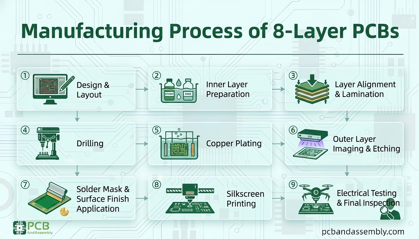
Understanding the manufacturing sequence helps designers make smarter DFM decisions and communicate effectively with fabricators:
① Design & Layout
Generate Gerber files, drill files, and a detailed stackup specification from the EDA tool. Verify all impedance-controlled traces meet calculated targets.
② Inner Layer Preparation
Each inner copper layer is imaged with the circuit pattern using photolithography, then chemically etched to remove unwanted copper, leaving only the desired traces, pads, and planes.
③ Layer Alignment & Lamination
Inner layers, prepreg sheets, and outer copper foil are precisely aligned using registration pins, then bonded under heat and pressure. The prepreg resin flows, encapsulates traces, and cures into a solid, void-free dielectric.
④ Drilling
CNC drilling creates through-holes for vias and component mounting. Laser drilling is used for microvias (blind vias) in HDI designs. Registration accuracy is critical here—misalignment can short traces to plane layers.
⑤ Copper Plating
Drilled holes are chemically seeded and then electroplated with copper to establish electrical conductivity between layers. Plating thickness typically targets 25 µm minimum in holes.
⑥ Outer Layer Imaging & Etching
The outer copper layers are imaged and etched to create the final surface circuit patterns, completing the full interconnect structure.
⑦ Solder Mask & Surface Finish Application
Solder mask is applied and cured to protect copper traces. The chosen surface finish (HASL, ENIG, or OSP) is then applied to exposed pads.
⑧ Silkscreen Printing
Component reference designators, polarity markers, and other assembly information are screen-printed for manufacturing and service use.
⑨ Electrical Testing & Final Inspection
Flying-probe or bed-of-nails testing verifies electrical continuity and isolation across all nets. Automated optical inspection (AOI) and, where required, X-ray inspection confirm inner layer integrity before shipment.
9. Applications of 8-Layer PCBs
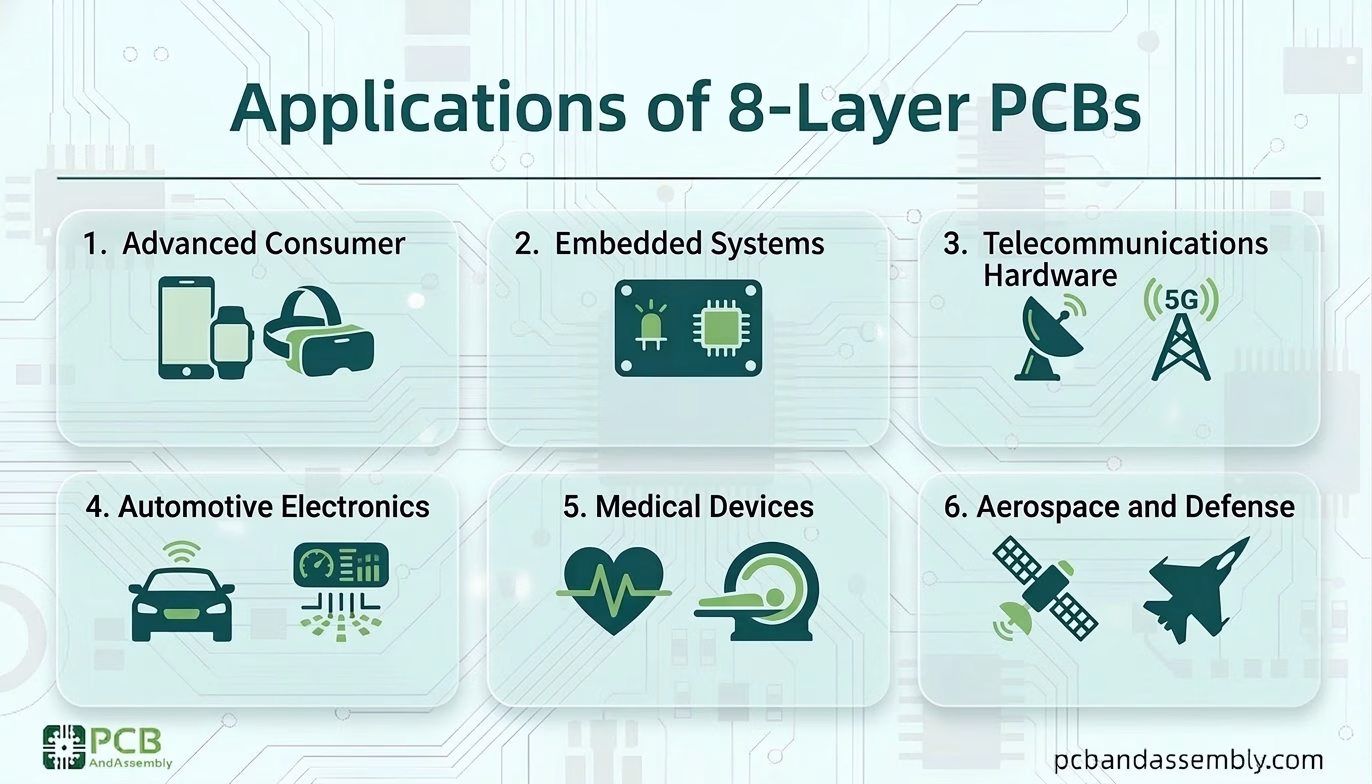
The versatility and robust performance of 8-layer PCB stackups make them suitable for a wide array of demanding electronic applications. They bridge the gap between simpler, lower-layer boards and highly specialized, very high-layer count designs, offering a sweet spot for many modern technologies:
- Advanced Consumer Electronics:High-end smartphones, tablets, laptops, gaming consoles, and smart home devices often utilize 8-layer PCBs for their compact size and ability to handle complex processors and high-speed data transfer.
- Embedded Systems:Industrial control systems, medical diagnostic equipment, network routers, and sophisticated sensors frequently rely on 8-layer designs to integrate various functionalities and ensure reliability in diverse operating environments.
- Telecommunications Hardware:Base stations, network switches, servers, and other communication equipment benefit from the excellent signal integrity and EMI performance of 8-layer PCBs, crucial for maintaining high data rates and reliable connectivity.
- Automotive Electronics:Advanced driver-assistance systems (ADAS), infotainment systems, engine control units (ECUs), and other critical automotive components require the robustness and performance that 8-layer stackups can provide.
- Medical Devices:Precision medical instruments, imaging equipment, and patient monitoring systems often incorporate 8-layer PCBs due to their ability to support complex signal processing and maintain high reliability for critical functions .
- Aerospace and Defense:Avionic systems, radar equipment, and guidance systems demand extremely high reliability and performance under harsh conditions, making 8-layer PCBs a common choice for these critical applications.
These applications underscore the importance of 8-layer PCB stackups in driving innovation across various industries, enabling faster, more powerful, and more reliable electronic devices.
10. Challenges of an 8-Layer PCB Stackup
While 8-layer PCBs offer clear performance advantages, designers and project managers should plan for the following considerations:
Higher Manufacturing Cost:
Additional layers require more materials, more process steps, and tighter tolerances—translating to higher fabrication cost compared to 4- or 6-layer boards. Evaluate whether the performance requirements genuinely justify the additional investment.
Longer Lead Time:
The increased process complexity (more lamination cycles, tighter alignment requirements) typically extends fabrication lead time. Factor this into project schedules.
Increased Testing Complexity:
Inner layer defects, via integrity issues, and impedance deviations are harder to detect and debug in 8-layer boards. Invest in simulation tools and work with manufacturers offering X-ray and controlled-impedance testing.
Limited Post-Fabrication Modifications:
Once laminated, 8-layer PCBs are extremely difficult to modify. Trace cuts and wire jumpers are limited to outer layers. Front-load the design review and simulation effort to minimize costly respins.
Increased Weight and Thickness:
Additional copper and dielectric material adds mass—a relevant constraint for aerospace, portable, and wearable applications where every gram matters.
11. FAQ
Q: What is the main advantage of an 8-layer PCB over a 4-layer PCB?
A: The main advantage is significantly improved signal integrity, power distribution, and EMI reduction due to the ability to include more dedicated ground and power planes. This allows for more complex routing of high-speed signals without compromising performance, which is difficult on a 4-layer board.
Q: How does an 8-layer stackup help with EMI reduction?
A: An 8-layer stackup typically places signal layers adjacent to solid ground or power planes. These planes act as effective shields, containing electromagnetic fields and providing clear, low-impedance return paths for signals. This arrangement greatly reduces both radiated and conducted EMI.
Q: Is an 8-layer PCB always better than a 6-layer PCB?
A: Not “always” in every scenario. For designs with moderate complexity, a well-designed 6-layer PCB can be very effective and more cost-efficient. However, for applications requiring higher signal speeds, more complex routing , or more stringent EMI control, an 8-layer PCB offers greater advantages and flexibility, making it the better choice for those specific needs.
Q: What types of motherboards typically use 8-layer PCBs?
A: High-performance computing motherboards—including gaming mainboards, workstation boards, and server platforms—commonly use 8-layer PCBs. These designs must handle multiple high-speed interfaces (PCIe Gen 4/5, DDR5, USB4) simultaneously, requiring the impedance control and crosstalk isolation that only a dedicated 8-layer stackup can reliably provide.
Q: When should I consider using blind or buried vias?
A: When routing density on outer layers is the primary bottleneck and the design budget allows for the additional manufacturing cost, blind and buried vias free up considerable outer-layer real estate. They are standard in HDI (High Density Interconnect) designs such as smartphones, where BGA pitch is below 0.5 mm and through-hole vias would consume excessive pad area.
12. Summary
The 8-layer PCB stackup represents a critical component in modern electronic design, providing an optimal balance between performance, functionality, and manufacturability. By comprising eight distinct layers, typically including four signal layers and four plane layers (ground and power ), it enables intricate routing while ensuring robust power distribution and superior signal integrity. Its advantages—such as enhanced EMI reduction, greater routing flexibility, and the ability to handle high-speed signals—make it indispensable for advanced consumer electronics, embedded systems, communication hardware, and a multitude of other demanding applications. Successful implementation hinges on adhering to best practices in PCB design, including meticulous impedance control, strategic power distribution network optimization, and proactive collaboration with PCB manufacturers. As electronic devices continue to push the boundaries of performance and miniaturization, the 8-layer PCB stackup will remain a cornerstone, empowering innovation across various industries.
Table of Contents
- 1. परिचय
- 2. 8-लेयर पीसीबी स्टैकअप क्या है?
- 3. 8-लेयर पीसीबी स्टैकअप क्यों चुनें?
- 4. 8-लेयर स्टैकअप के प्रमुख घटक
- 5. सामान्य 8-परत स्टैकअप कॉन्फ़िगरेशन
- कॉन्फ़िगरेशन 3: ग्राउंड–सिग्नल–ग्राउंड–सिग्नल–सिग्नल–पावर–सिग्नल–ग्राउंड
- 6. बोर्ड की मोटाई और परत के आयाम
- 7आवश्यक डिज़ाइन दिशानिर्देश और सर्वोत्तम अभ्यास
- 8. 8-लेयर पीसीबी की निर्माण प्रक्रिया
- 98-लेयर पीसीबी के अनुप्रयोग
- 10. 8-लेयर पीसीबी स्टैकअप की चुनौतियाँ
- 11. सामान्य प्रश्न
- 12। सारांश

Get Your PCB Quote!