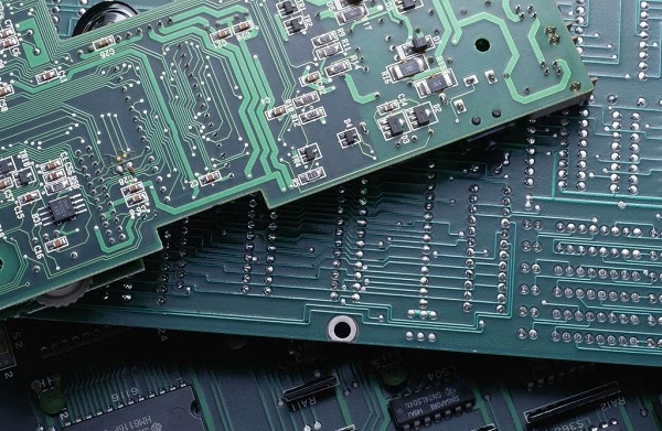
Impedance Control PCB Prototyping & Manufacturing
PCBAndAssembly provides PCB manufacturing and prototyping services with a focus on controlled impedance to support high-speed signal performance. Controlled impedance ensures signal integrity in high-speed PCB designs by maintaining consistent impedance throughout traces. We design printed circuit boards with impedance requirements tailored for reliable performance in RF, high-speed digital, and mixed-signal applications.
ISO 9001/UL Certified
PCB Assembly Specialists
On Time Delivery 98.15%
Quality Pass Rate 99%
Delivery Guarantee
ISO 9001/UL Certified
PCB Assembly Specialists
On Time Delivery 98.15%
Quality Pass Rate 99%
Delivery Guarantee
What is Impedance Control in PCB?
Impedance is a measure of the total opposition that a circuit presents to alternating current (AC) when a voltage is applied. An impedance value is usually represented by the symbol Z and is measured in ohms (Ω). Moreover, impedance is an important concept in electrical engineering and electronics.
As electronic devices advance, they use more powerful components and drivers that communicate through high-power, high-frequency signals. Traditional copper signal trace designs are not capable of handling this performance. However, you can design a controlled impedance PCB to take care of this.
With PCB-controlled impedance, you get several improvements, such as thicker and wider copper traces to transmit high-speed signals. At PCBAndAssembly, our manufacturing process places a focus on controlled impedance designs to ensure optimal performance for high-speed applications. If you’re interested in our services, feel free to request a PCB assembly quote to learn more!
Standard impedance value used in many high-frequency applications, including radio frequency (RF) circuits and test equipment
Used in video and cable television applications
Often used in differential impedance signaling applications, such as Ethernet and USB
Used in some antenna systems and older television applications
How to Achieve Impedance Controlled PCBs
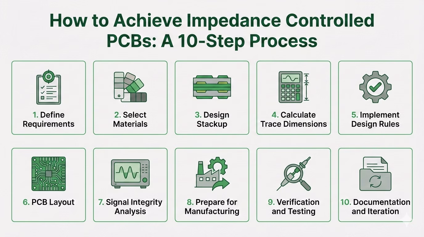
1. Define Controlled Impedance Requirements
The first step is to define your impedance target. For single-ended traces on the PCB, the most common values are 50 Ω, 75 Ω, and 100 Ω. Differential pairs are 90 Ω, 100 Ω, and 120 Ω. Then, you’re going to have to determine the frequency range of operation, as this affects the material selection and design rules.
2. Select Appropriate Materials
It’s important to choose the right PCB stackup. Select FR-4 for lower frequencies, but select high-frequency laminates for RF applications.
Lower dielectric constant (Dk) materials typically offer improved performance, while lower dissipation factor (Df) reduces signal loss. Then, be sure to choose the correct copper weight, often between 0.5 to 2 oz per square foot
3. Design the PCB Stackup
Start by figuring out how many layers you’ll need; more layers provide you with better control, but they also increase the cost.
Arrange the signal and plane layers, typically as signal-ground-power-signal. Then, you’ll calculate the dielectric thickness using impedance calculators or specialized software. For more complex designs, you might want to use buried and blind vias.
4. Calculate Trace Dimensions
Use impedance calculation formulas or software to calculate trace dimensions. You’ll need to determine trace width and spacing and adjust these to calculate the impedance value. Also, keep in mind manufacturing tolerances. If you have differential pairs, you’ll have to calculate the individual trace width and the spacing between traces.
5. Implement Design Rules
Set up the trace width and spacing rules in your CAD software and define size, spacing, and type via routes. Then you need to establish clearance rules for between traces, pads, and planes. Create length-matching rules for differential pairs.
6. PCB Layout
Place components to minimize critical trace lengths. Route critical signals first with consistent width and smooth bends. Use reference planes for return paths and route differential pairs as parallel, equal-length traces with length matching. Finally, add guard traces and stitching vias to control crosstalk.
7. Signal Integrity Analysis
Start by performing a pre-layout simulation using tools like HyperLynx or HFSS. Then, conduct a post-layout simulation to verify impedance control and make sure to check for reflections, crosstalk, and EMI issues.
Analyze eye diagrams to ensure that signal quality meets specifications and iterate design if necessary by adjusting trace widths, spacings, or stackup.
8. Prepare for Manufacturing
Generate accurate Gerber files and include impedance requirements in fabrication notes. Specify impedance control requirements, including target impedances for different trace types and acceptable tolerance ranges.
Then, request impedance coupons and test structures for impedance verification. Finally, choose a PCB manufacturer experienced in characteristic impedance control, like OurPCB.
9. Verification and Testing
Perform Time Domain Reflectometry (TDR) measurements to verify actual trace impedance. Use Vector Network Analyzer (VNA) for high-frequency testing to measure S-parameters. Then, conduct functional testing to ensure the PCB meets performance requirements. Analyze test results and make adjustments if necessary.
10. Documentation and Iteration
- Document all design decisions and test results
- Create a report detailing impedance control achievements
- Use insights gained to improve future designs
- Consider creating design guidelines for your organization
PCB Assembly Services
Turnkey PCB Assembly
We handle everything from parts sourcing to final assembly, providing a hassle-free experience that ensures top-quality boards every time.
Prototype & Full Production Runs
Whether you need a few prototypes or large-volume batches, our flexible assembly services adapt to your project’s scope and timeline.
RoHS & Lead-Free Compliance
Stay environmentally responsible with our compliant assembly processes, offering RoHS and lead-free options for safe, reliable builds.
Single-Sided, Double-Sided, or Mixed
No matter the complexity, we can assemble boards of all configurations—single-layer, multi-layer, or a mix—to match your exact specifications.
Small Quantities & High-Volume Capabilities
From one-off prototypes to bulk orders, we accommodate projects of all sizes without compromising on quality or turnaround time.
Trusted by Over 3,000 Customers Worldwide
Join our growing community of satisfied clients who rely on our dependable assembly expertise and dedicated customer support.
Technical Capabilities

Capabilities & Services
PCB Factory Gallery