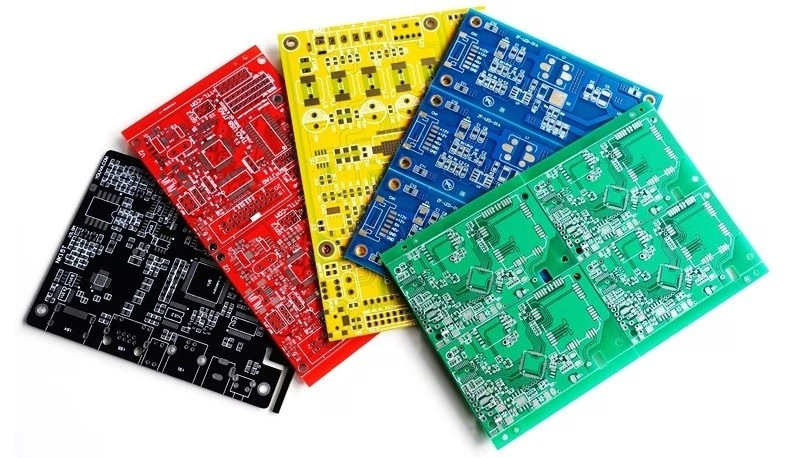
Flexible PCB Assembly
If you are looking for a reliable flexible or rigid-flex PCB manufacturer, PCBAndAssembly provides high-quality custom solutions for original equipment manufacturers (OEMs) with fast delivery to the United States and worldwide. Our services cover various industries, including automotive, medical devices, and consumer electronics.
Introduction to Flexible Printed Circuit Boards
A flexible printed circuit board (flex PCB or flex circuit) is a type of printed circuit board that is made of flexible insulating material such as polyimide film. Unlike traditional rigid PCBs, flex PCBs can bend and flex while still maintaining their electrical connectivity. Some key advantages of using flex PCBs include:
- Ability to bend and flex to fit mechanically challenging spaces
- Lightweight and thin profile
- Good for high density interconnected assemblies
- Can be folded and wrapped around edges
- Resistant to vibration and fatigue
- Often used in smaller consumer electronics
Flex PCB Assembly Process Steps Explained
Our Flexible PCB Manufacturing Capability
Below is a detailed overview of our Flex & Rigid-Flex PCB capabilities, showcasing the key specifications and performance metrics that highlight our commitment to precision and quality in every project.
| Project Item | Normal Capability |
| FPC Base Material (Adhesive) | ShengyiSF302:PI=0.5 mil,1 mil,2 mil;Cu=0.5 oz,1 oz ShengyiSF305:PI=0.5 mil,1 mil,2 mil;Cu=0.33 oz,0.5 oz,1 oz |
| FPC Base Material (Adhesiveless) | SongxiaRF-775/777:PI=1 mil,2 mil,3 mil;Cu=0.5 oz, 1 oz (Ultimate:PI=1 mil,2 mil,3 mil;Cu=2 oz) Xinyang:PI=1 mil, 2 mil;Cu=0.33 oz, 0.5 oz, 1 oz Taihong PI=1 mil, 2 mil;Cu=0.33 oz, 0.5 oz, 1 oz Dubang AP:PI=1 mil, 2 mil, 3 mil, 4 mil;Cu=0.5 oz, 1 oz (Ultimate:PI=1 mil,2 mil,3 mil,4 mil;Cu=2 oz) |
| Layer | 1-6 Layers (Ultimate:7-10 Layers) |
| Thickness of Finished Product (Flex part,no stiffener) | 0.05-0.5 mm (Ultimate: 0.5- 0.8 mm) |
| Size of Finished Products(Min) | 5 mm*10 mm (Bridgeless);10 mm*10 mm (Bridge) Ultimate:4 mm*8 mm (Bridgeless);8 mm*8 mm (Bridge) |
| Size of Finished Products (Max) | 9 inch*14 inch Ultimate:9 inch*23 inch (PI≥1 mil) |
| Impedance Tolerance | Single-Ended:±5Ω(≤50Ω),±10%(>50Ω) Ultimate:Single-Ended:±3Ω(≤50Ω),±8%(>50Ω) |
| Impedance Tolerance | Differencial:±5Ω(≤50Ω),±10%(>50Ω) Ultimate:Differencial:±4Ω(≤50Ω),±8%(>50Ω) |
| Tolerance of Finger Width | ±0.1 mm (Ultimate:±0.05 mm) |
| Min Distance to the Edge of Finger | 8 mil (Ultimate:6 mil) |
| Min Distance between Pads | 4 mil (Ultimate:3 mil) |
| Minimum Laser Hole | 0.1mm |
| Minimum PTH | 0.3mm |
| Min NPTH Tolerance | ±2 mil (Ultimate +0,-2 mil or +2 mil,-0) |
| Solder Bridge Min Width(bottom copper<2OZ) | 4 mil(Green),8 mil |
| Solder Bridge Min Width(bottom copper 2-4OZ) | 6 mil,8 mil |
| Overlay Colour | White、Yellow (printed character:White) |
| Type of Surface Treatment | OSP HASL, Lead free HASL, Immersion gold, Hard gold, Immersion silver, OSP |
| Selective Surface Treatment | ENIG+OSP,ENIG+G/F |
Our Rigid-Flex PCB Manufacturing Capability
| Project Item | Normal Capability |
| FPC Base Material (Adhesive) | Shengyi SF302, Shengyi SF305 |
| FPC Base Material(Adhesiveless) | Songxia RF-775/777, Xinyang, Dubang AP |
| Low flow prepreg | Taiguang EM-37B; Ventec: VT-47N |
| Common rigid board material | Refer to standard rigid board materials |
| Special rigid board material | Arlon: 85N; Rogers: RO4000 series; Nelco: N4000-13 series; Ventec: VT-901 |
| Layer | 2-30 Layers; review required: ≥20 layers |
| Thickness of Finished Product | 0.3-4.0mm; review required: >3.0 mm |
| Size of Finished Products(Min) | 10mm*15mm (no internal positioning designs, panel size <50mm*50mm) |
| Size of Finished Products (Max) | 18inch*22inch; Ultimate:18inch*29inch |
What is the Cost of Flexible PCBs?
On average, flexible PCBs can range from $0.50 to $5.00 per square inch for standard designs and materials. However, this cost is not fixed and can vary based on several factors. The factors that influence the price include necessary assembly labor, prevailing labor rates, and the time required for assembly. Additionally, overhead manufacturing expenses and the design complexity of the board play significant roles in determining the final cost. To get a more accurate cost estimate, please use our free pcb quote form.
Factors Affecting Flex & Rigid-Flex PCB Costs
- Physical Size: Larger PCBs cost more, calculated per square inch.
- Circuit Construction: Costs depend on materials, layers, and pads. Extra layers or high-quality materials increase costs.
- Volume: Higher volumes result in higher costs.
- Layers: More layers mean higher assembly costs. Opt for single-sided FPCBs if possible.
- Finishing: Premium finishes guarantee longevity but come at a higher price.
- Holes: More or smaller holes drive up costs due to increased drilling complexity.
- Flex Board Types: Layer count influences price significantly.
- Custom Features: Specifications like solder mask clearance, side plating, or contoured edges add to the cost.
How to Reduce PCB Production Costs
- Minimize flexible layers, as rigid laminates are more cost-effective.
- Reduce overall layers to lower the need for additional materials.
- Limit controlled impedance requirements to necessary values only.
- Opt for flexible copper thickness, approximately 1/3 oz.
- Purchase FPCBs in bulk to reduce unit cost.
Flexible & Rigid-Flex PCB Lead Times Overview
| Service Type | Lead Time |
| Standard PCB Manufacturing | 5-6 days |
| Expedited Manufacturing | 24-48 hours |
| PCB Prototyping (Quick Turn) | 1-12 layers: within 72 hours |
| 12+ layers: within 120 hours | |
| PCB Assembly | 4-25 days, depending on complexity and order volume |

