Shenzhen SMT Patch Processing Technology
Get Your PCB Quote!
Table of Contents
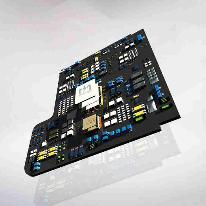
SMT is the most popular processing technology in the current electronic assembly industry. It can save costs and time to a great extent and improve production efficiency. This processing technology has been used in the processing plant of pcbandassembly Technology. SMT can be divided into single-sided and double-sided patch processing technologies, and can also be divided into assembly and mixed assembly. Today, I will show you how to do it.
Single-Sided Assembly:
Incoming material inspection → Screen printing solder paste (apply SMD glue) → SMD → Drying (curing) → Reflow soldering → Cleaning → Inspection → Rework
Double-Sided Assembly:
A: Incoming material inspection → Screen printing solder paste (apply SMD glue) on PCB A side → Screen printing solder paste (apply SMD glue) on PCB B side → SMD → Drying → Reflow soldering (preferably only on B side → Cleaning → Inspection → Rework).
B: Incoming material inspection → Screen printing solder paste (apply SMD glue) on PCB A side → SMD → Drying (curing) → Reflow soldering on A side → Cleaning → Flip board → Apply SMD glue on PCB B side → SMD → Curing → Wave soldering on B side → Cleaning → Inspection → Rework.
This processing technology is suitable for reflow soldering on the PCB A side and wave soldering on the B side. This processing technology is suitable for SMDs assembled on the PCB B side when there are only SOT or SOIC (28) pins or less.
Single-Sided Mixed Assembly:
Incoming material inspection → Screen printing solder paste on PCB A side (applying SMD glue) → SMD → Drying (curing) → Reflow soldering → Cleaning → Insertion → Wave soldering → Cleaning → Inspection → Rework
Double-sided mixed assembly:
A: Incoming material inspection → Apply SMD glue on PCB B side → SMD → Curing → Flip board → Insertion on PCB A side → Wave soldering → Cleaning → Inspection → Rework
Apply first and then insert, suitable for the situation where there are more SMD components than discrete components
B: Incoming material inspection → PCB A Surface plug-in (pin bending) → flip board → PCB B surface SMD glue → SMD → curing → flip board → wave soldering → cleaning → inspection → rework
Plug in first and then stick, suitable for the situation where there are more discrete components than SMD components
C: Incoming material inspection → PCB A surface screen printing solder paste → SMD → drying → reflow soldering → plugin, pin bending → flip board → PCB B surface SMD glue → SMD → curing → flip board → wave soldering → cleaning → inspection → rework A surface mixed, B surface mounting.
D: Incoming material inspection → PCB B surface SMD glue → SMD → curing → flip board → PCB A surface screen printing solder paste → SMD → A surface reflow soldering → plugin → B surface wave soldering → cleaning → inspection → rework A surface mixed, B surface mounting. First, paste SMD on both sides, reflow soldering, then insert and wave soldering
E: Incoming material inspection => PCB B side screen printing solder paste (apply SMD glue) → SMD → drying (curing) → reflow soldering → (local soldering can be used) → plug-in → wave soldering 2 (if there are few insert components, manual soldering can be used) → cleaning → inspection → rework A side mounting, B side mixed assembly.
The above is the single-sided and double-sided patch process of Shenzhen SMT processing. You are welcome to contact pcbandassembly Prototyping at any time and visit the factory for consultation. Pcbandassembly has 6 years of SMT processing experience in Shenzhen, with high product quality and fast delivery.
Shenzhen pcbandassembly, a long-established electronic processing factory in Shenzhen, can provide SMT processing services. It also has rich experience in PCBA processing. PCBA is a one-stop service for you. pcbandassembly can also undertake DIP plug-in processing, PCB production, and electronic circuit board manufacturing services.
Table of Contents
Get Your PCB Quote!

