How to Solder Castellated Holes in PCB Design?
The guide delves into castellated mounting holes, exploring their design principles, advantages, manufacturing complexities and best practices for soldering.
Get Your PCB Quote!
Table of Contents
Table of Contents
Castellated holes are plated half-holes with their centers on the board edge, used to solder a small module board flat onto a larger motherboard like an SMD component. Most design guides stop at a definition and a minimum drill size, which misses the part that actually decides whether your module ships working: the joint has to form inside a half-cylinder of copper, and every rule that governs how that hole is designed, cut, and finished shows up later as a solder defect or a clean joint. This guide covers the design rules with real numbers, the soldering process for both hand and production work, and what a good joint looks like when you inspect it.
Quick Specs: Castellated Holes at a Glance
|
What they are |
Plated through-holes with centers on the board outline, milled in half to leave a plated half-cylinder on the edge |
|
Used for |
Board-to-board mounting of Wi-Fi, Bluetooth, NB-IoT and other modules as SMD-like components |
|
Minimum drill diameter |
0.6mm (JLCPCB) to 0.8mm (Eurocircuits); recommended 0.8-1.0mm |
|
Recommended pad size |
Drill diameter + 0.70mm |
|
Annular ring |
0.25mm minimum (0.18mm absolute limit) |
|
Hole-to-hole clearance |
0.6mm minimum; 0.8mm recommended |
|
Board edge to pad |
1.0mm minimum |
|
Surface finish |
ENIG recommended; mandatory when slot length is 5mm or longer |
|
Minimum board size |
10mm x 10mm; panelize below 20mm |
|
Panel rule |
V-cut is forbidden on castellated edges; CNC milling only |
Key Takeaways
- A castellated hole is a PTH drilled with its center on the board outline and then milled in half, so the design rules that keep the plating intact (0.6-1.0mm drill, 0.25mm ring, 1.0mm edge clearance, PTH not NPTH) decide whether the joint can ever form.
- Two fabricators quote different minimums: JLCPCB accepts 0.6mm drill while Eurocircuits requires 0.8mm. Design at 0.8-1.0mm and you satisfy both, and the extra copper makes the half-wall less likely to peel.
- Castellated boards cost more because the final routing step is a controlled two-step drill-and-mill sequence that keeps the half-cylinder from lifting; the premium buys plating integrity, not speed.
- V-cut scoring is forbidden on any edge with castellations. The V-cut tool pulls the copper away from the hole wall, so castellated edges are always CNC milled.
- Hand soldering works at 370°C with a small tip, flux on every joint, and a five-pass routine: tin one corner pad, slide the module into the molten solder, then work along the row. Bridges are fixed with flux and solder wick, never by adding more solder.
What castellated holes are, and where they earn their place
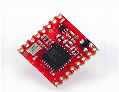
A castellated hole, also called a plated half-hole or castellation, is a plated through-hole whose center sits exactly on the board outline. The fabricator drills a normal PTH, plates it, then mills the board edge so the outer half of the barrel is removed, leaving a plated half-cylinder exposed on the edge. A row of these forms a castellated edge, and the module solders to a host board through those half-cylinders exactly the way a surface-mount package solders to its pads.
The main use is board-to-board mounting of pre-built modules. Wi-Fi, Bluetooth, NB-IoT, RF transceivers, and other radio modules ship as small boards with a castellated edge on one or two sides, and a host product solders them flat onto its own board. The half-holes give the assembly process three advantages over bottom-side pads: the joints are visible and accessible for inspection, the holes self-align the module during placement, and you can measure the solder coverage with calipers after assembly, which you cannot do with pads hidden under the module.
Castellated mounting is not a one-off trick. It is a production-grade joining method that runs through standard SMT lines, which is why module vendors and OEMs both favor it: the module behaves like a component in the pick-and-place and reflow process. When the joint is well designed, the mechanical strength comes from the plated barrel bonded to the pad, and the electrical path is short and direct to the host board’s traces.
Point to remember: castellations trade reworkability for density. The joint is permanent, so use them when the module will never need removal; if a module might be swapped in the field, a connector or socket is the safer choice, and section on alternatives covers that decision.
Six design rules that decide whether your joint ever forms
The solder joint is only as good as the half-cylinder it forms inside, so the design rules come first, before any iron is involved. These six parameters are what the fabricator checks in the CAM stage, and they are the ones that cause engineering queries when you get them wrong. They matter because a half-wall that is too thin, too close to another hole, or plated on an NPTH will fail before you ever open a solder spool.
Castellated hole design rules: fabricator minimums and recommended values
| Parameter | minimum | Eurocircuits minimum | Recommended design value |
| Drill diameter | 0.6mm | 0.8mm | 0.8-1.0mm |
| Pad size | drill + ring | drill + 0.70mm | drill + 0.70mm |
| Annular ring | 0.25mm (0.18mm abs.) | — | 0.25mm |
| Hole-to-hole clearance | 0.6mm | — | 0.8mm |
| Board edge to pad | 1.0mm | — | 1.0mm |
| Pad inward extension | 0.5mm | — | 0.8mm |
| Hole to board corner | 3.0mm | — | 5.0mm |
| Surface finish | ENIG (mandatory if slot ≥ 5mm) | ENIG recommended | ENIG |
The most useful number in the table is the drill diameter, and it is also the one where the two fabricators disagree: JLCPCB accepts 0.6mm as a minimum while Eurocircuits will not go below 0.8mm. Both are telling the truth about their own process. Design at 0.8-1.0mm and you clear both bars, and the larger barrel gives you a bigger soldering target and a half-wall that resists peeling during the milling step.
Three rules in that table trip people up more than the rest. First, the pad must extend inward at least 0.5mm from the board edge, because that copper is what anchors the half-wall to the laminate; without it, routing torque peels the plating. Second, the hole has to be defined as a plated through-hole (PTH) in the EDA tool. If it is marked NPTH, the fabricator follows the file and mills away the copper, leaving a bare half-hole that will not accept solder. Third, the board outline must cut through the exact centerline of the holes, which is how the tool knows it is a castellated edge at all.
For a 0.8mm drill diameter, the recommended pad is drill + 0.70mm = 1.50mm. With a 0.25mm annular ring, that leaves the pad extending 0.35mm past the hole wall on each side, which clears the 0.5mm inward-extension rule when the pad sits flush with the board edge. If you drop to a 0.6mm drill, the same +0.70mm rule gives a 1.30mm pad, and the ring drops to 0.35mm total width, which is why the 0.8mm design is the safer starting point.
Surface finish is not optional here. The half-wall is bare copper inside, and bare copper oxidizes in hours, so the plating needs an organic or metallic finish that survives storage and the first reflow. ENIG is the standard recommendation, and it becomes mandatory once any slot on the edge is 5mm or longer, because a long slot has more exposed copper surface to protect.
Decision rule: design castellated holes at 0.8-1.0mm drill, 0.25mm ring, 1.0mm edge clearance, and ENIG finish, and you will pass every fabricator’s CAM check on the first pass.
Why castellated boards cost more (and what the premium buys)
A castellated board carries a price premium over the same board with a plain edge, and the reason is mechanical, not commercial. The fabricator cannot just route the outline and ship: the copper plating inside the half-cylinder has to survive the cut, and a standard single-pass routing tool tends to tear it off.
The mechanism is easy to visualize. The routing spindle rotates clockwise. Where the tool enters the hole wall, the cutter pushes the copper against the laminate and the plating stays put. On the opposite side, where the copper has no backing, the tool’s rotation curls the plating up, leaving a burr or peeling the barrel entirely. To avoid that, castellated production runs a two-step sequence: drill and plate the holes first, then a controlled CNC profile-milling pass that cuts the barrels in half while keeping the plating intact, followed by deburring and inspection. That extra pass, plus the CAM work to program the tool path, is what the premium pays for.
Two more cost drivers come with the design. Small modules below 20mm have to be panelized for safe handling during routing, and the panel layout with its breakaway tabs and mouse-bite holes adds material and routing time. And ENIG, the required finish, costs more per square meter than HASL or OSP, a difference that shows up on any small board where finish is priced by area.
So when a quote for a castellated board comes in noticeably higher than a plain-edge prototype of the same size, that is the two-step routing sequence and the finish, not margin. The premium buys plating integrity, and plating integrity is what turns a module edge into a solderable surface instead of a row of shredded copper.
Point to remember: ask what the premium covers. A shop that quotes a castellated premium but cannot describe its routing sequence is likely running a standard pass and shipping whatever survives it.
Panelizing an edge that cannot be V-scored
Castellated edges and V-cut scoring do not mix, and this is the rule that catches more first-time designs than any other. A V-cut tool scores a groove into the board and snaps the panel apart, and that pull is exactly what peels the plating off a half-cylinder. Every fabricator that documents the rule says the same thing: no V-cut on any edge that carries castellations. Those edges are CNC milled, and the rest of the panel can use whatever method the design allows.
For panels, the practical options are mouse-bite (stamp hole) breakaway tabs, and the tab geometry matters because the tabs are where the module gets its mechanical strength during routing and separation. The fabricator needs enough material between the stamp holes and the castellated pads so the stress of breaking the tabs does not crack a plated barrel.
Mouse-bite panelization for castellated modules
| Parameter | Recommended value |
| Stamp hole drill size | 0.5-0.8mm (0.6mm typical) |
| Stamp hole spacing (center to center) | 1.0-1.2mm |
| Holes per breakaway tab | 4-6 |
| Clearance from stamp hole to castellated pad | 1.0mm minimum |
| Breakaway tab width | 5mm per side (Eurocircuits guidance) |
| Minimum panel dimension | 10mm |
The EDA setup for panelization has to match what the fabricator expects. The board outline layer (Edge.Cuts in KiCad, Mechanical 1 or Keep-Out in Altium) must bisect the castellated holes exactly down their centerline, the holes must be PTH, and the associated copper pads must extend inward past the outline. If the outline does not cut the holes, the CAM tool does not recognize them as castellations and the whole feature is misread at the start of the job.
Decision rule: keep castellations off any V-scored edge, use mouse-bite tabs with 1.0mm clearance to the nearest pad, and make sure the board outline bisects the holes down the centerline.
Hand soldering a castellated module: a five-pass routine
Hand soldering a castellated module is straightforward once the design is right, and the tool list is short. The critical numbers are the iron temperature, 370°C (about 700°F), and the tip size: the tip has to fit on one pad without spanning two, because a wide tip is how bridges happen. Use lead-free solder with a flux core around 0.020″ diameter, keep a flux pen and solder wick on the bench, and have a stiff brush and isopropyl alcohol ready for cleanup.
The routine is five passes, and each one has a purpose:
1. Tin the first corner pad. Pick the pad at one end of the row, hold the iron on it for one to two seconds, and feed solder until a small mound forms. This anchor pad is what holds the module in place while you work the rest.
2. Add flux to the tinned pad. The flux in the solder core burned off when you melted it, so the mound needs fresh flux before it can be reheated and accept the module. A flux pen over the mound is enough.
3. Slide the module into the molten mound. Hold the module with tweezers, reheat the mound, and slide the module into place while the solder is liquid. The castellation should touch the pad, and the solder should wick up into the half-cylinder. Check the module orientation before you commit; a reversed RF module is the classic way to spend an afternoon fixing a mistake that was visible for the five seconds before the solder set.
4. Solder the remaining pads one at a time. For each pad, touch the iron tip to both the castellation and the pad, feed solder into the joint, and wait for it to wet the half-wall. Remove the solder first, then the iron, and let each joint cool before touching it.
5. Clean and inspect. Scrub the flux residue off with the brush and isopropyl alcohol, then check every joint: solder should cover the castellation and the pad with a bright, concave fillet.
Two behaviors in this routine will save you the most grief. First, pads connected to a ground plane or power pour are stubborn: the copper pours away heat faster than a trace, so those joints need a few extra seconds of heat and a little extra flux. Second, if a bridge forms between two holes, the fix is flux plus solder wick, not more solder. Lay the wick over the bridge, touch the iron to the wick, and the excess solder gets drawn off.
Point to remember: the anchor-pad trick, tin one corner first and slide the module into the molten solder, is what keeps the module aligned through the whole row. Soldering the row in sequence without an anchor is how modules end up crooked.
Production soldering: stencil wells, paste, and reflow
Hand soldering covers prototypes and repairs, but production castellated modules run through the same SMT line as everything else: stencil, paste, placement, reflow, inspection. The difference from a normal SMD pad is that the joint must form up the side of the half-cylinder, so the paste volume and the pad geometry have to give the solder somewhere to go.
The stencil is where that gets tuned. The pad on the host board should be at least as long as the module’s half-wall so the joint has vertical area to climb, and the stencil aperture can be sized to deposit a bit more paste than a same-area standard pad, because part of the paste wicks up the wall instead of staying flat on the pad.
The reflow profile itself is the same lead-free curve the rest of the board uses, with the peak temperature and time-above-liquidus driven by the solder paste you choose, and our solder paste guide covers the composition and printing considerations that matter here. What differs is inspection: castellated joints are checked from the edge, not from above, so the AOI program has to include a side-view or angled check on the castellated row, something a default top-down AOI setup does not do.
Placement accuracy also matters more than for a normal part. The module has to land so each half-cylinder sits centered on its pad; offset placement leaves one side of the wall unwetted, which reads as a cold joint under X-ray even when the paste printed cleanly.
⚠️ Important
The stencil and inspection recommendations above are engineering practice rather than a published standard, so confirm the aperture sizing with your assembler’s process team before committing a production stencil. The design rules in the earlier table are fabricator-documented; this section is the part of the process where the shop’s experience sets the final numbers.
Point to remember: production soldering of castellations is a stencil problem first and a placement problem second. Give the joint paste to climb with, land the module centered, and inspect from the edge.
Inspecting the joint: what good looks like and three failure modes
A good castellated joint is easy to recognize: solder fills the half-cylinder and wets up the wall, forming a smooth concave fillet between the castellation and the host pad, with no gap at the top of the barrel and no solder creeping past the pad onto the board edge. The solder surface is bright and continuous, and the module sits flush against the host board with no visible tilt.
Against that reference, three failure modes cover nearly everything that goes wrong, and each has a distinct cause and a distinct look.
Castellated joint failure modes
| Failure | What it looks like | Cause | Watch out for |
| Solder bridge | Solder connects two adjacent half-cylinders | Wide iron tip, excess paste, pads too close together | Fix with flux and wick; prevent with 0.8mm hole spacing and a small tip |
| Cold joint / poor wetting | Solder balled up or flat on the pad, not climbing the wall; dull surface | Insufficient heat, missing flux, oxidized half-wall, module placed off-center | Check pad connected to ground plane; add heat and flux; verify ENIG finish |
| Copper peeling / missing wall | Half-cylinder missing or ragged, bare laminate visible | Routing torque lifted the plating during milling | Design-side: PTH, 0.5mm pad extension, 0.8mm+ drill; caught at incoming inspection |
Bridges are the most common hand-soldering defect and the easiest to fix, which is why the routine above saves the anchor pad and the wick for the end. Cold joints are the production defect that inspection exists to catch, because a joint that never wet the wall looks fine from the top and fails intermittently in the field. And peeled copper is not a soldering defect at all: it is a fabrication defect that incoming inspection should catch before any solder is applied, which is why the incoming check matters on a castellated module.
For production acceptance, the visual criteria follow the same structure as any SMD joint: IPC-A-610J defines the acceptable wetting and fillet conditions, and the IPC J-STD-001J soldering requirements cover the process that produces them. Your assembler should be able to state which acceptance class they build and inspect to before you place the order.
Decision rule: inspect every castellated joint for wall coverage and fillet shape, treat bridges as a process fix rather than a rework problem, and reject any module whose half-wall shows peeling at incoming inspection, because that copper is gone before soldering starts.
When headers, fingers, or flex beat a castellated edge
Castellations are the right answer for a specific problem: permanent, low-profile, high-density board-to-board mounting of a module that will never come off. They are not the right answer for everything, and choosing the wrong joining method is one of the more expensive design mistakes in this area, because it is decided once and lived with for the product’s life.
Joining method comparison for module-to-board connections
| Method | Best for | Watch out for |
| Castellated edge | Permanent module mounting, production SMT line, tight height and space budgets, RF modules that need short connections | Not reworkable; edge must be CNC milled, no V-cut; ENIG finish required |
| Pin headers / sockets | Modules that get swapped, replaced, or upgraded; debug and evaluation boards | Height and footprint; two connectors in series add resistance and failure points |
| Edge fingers / board-edge connector | High insertion-cycle applications, standardized mezzanine interfaces | Cost of gold fingers and connector; needs board-edge real estate |
| FPC / flex cable | Modules at an angle or in a different plane, moving assemblies | Cable cost, connector cost, mechanical retention; another failure point in the chain |
| Through-hole pins (wave) | Maximum mechanical strength, vibration-heavy environments | Height, assembly cost, footprint; defeats the low-profile goal |
The decision mostly comes down to three questions: does the module ever need to come off, how much height and area can the product afford, and is the product built on an SMT line at volume? Castellations win when the answer is no, tight, and yes. If the module needs field replacement, a socket or header wins even though it costs height, because the service cost of replacing a soldered module in the field dwarfs the connector price. If the connection must flex or cross planes, a cable wins. If the board will live in a vibration environment, through-hole pins or a locked connector beat a solder joint, because a castellated joint has no mechanical latch to hold it.
Decision rule: use castellations when the module is permanent, space is tight, and the line is SMT; switch to a socket or header the moment field replacement is a requirement, because a soldered module with no removal path becomes a service problem.
Getting the quote right: nine checks before you send files
The castellated edge is the kind of feature that generates engineering queries if the file package is ambiguous, and every round-trip costs days. Run through these nine checks before you submit, and most of the back-and-forth disappears.
Quote-ready checklist for castellated boards
| # | Check | Why it matters |
| 1 | Holes set as PTH, not NPTH | NPTH gets milled clean, leaving an unsolderable half-hole |
| 2 | Board outline bisects hole centerlines | CAM recognition of the castellated feature depends on it |
| 3 | Pads extend inward at least 0.5mm past the outline | Anchors the plating against routing torque |
| 4 | 0.8-1.0mm drill diameter | Clears every fabricator’s minimum; bigger barrel solders better |
| 5 | 0.25mm annular ring and 0.8mm hole spacing | Prevents web cracking and solder bridges |
| 6 | ENIG finish selected, mandatory if any slot is 5mm+ | Protects the exposed half-wall copper |
| 7 | No V-cut on castellated edges; mouse-bite tabs with 1.0mm clearance | V-cut peels plating; stamp holes near pads crack barrels |
| 8 | Panelized if module is under 20mm | Small boards need safe handling during routing |
| 9 | Written confirmation of the routing sequence and deburring | Verifies the shop actually runs the two-step process |
On the last check, the phrasing matters. A simple “can you do castellated holes?” gets a yes from everyone; the useful question is “which edge finish and routing sequence do you use for castellated edges, and do you deburr and inspect after milling?” The answer tells you whether you are dealing with a real castellated process or a standard router running on hope.
It is also worth asking for the cost breakdown up front, because the castellated premium should be visible as a line item. If a quote does not show a separate charge for the half-hole process, either the shop is absorbing it (rare) or it is running a standard routing pass on your castellated board (common and bad).
Decision rule: the quote is not real until the shop confirms its routing sequence and deburring step in writing. Everything else in the checklist is a file correction; that one is a process verification.
FAQ
What is the minimum size for a castellated hole?
The minimum drill diameter ranges from 0.6mm to 0.8mm. Design at 0.8-1.0mm to clear both minimums, with an annular ring of at least 0.25mm and 0.8mm spacing between holes.
Why are castellated PCBs more expensive?
Castellated edges need a controlled two-step drill-and-mill sequence so the routing tool does not peel the plated half-wall, plus ENIG finish and panelization for small modules. The premium covers plating integrity, not margin.
Can I V-score a panel that has castellated holes?
No. V-cut scoring is forbidden on any edge that carries castellations, because the V-cut tool pulls the copper away from the hole wall. Castellated edges must be CNC milled, and breakaway tabs should use mouse-bite holes with 1.0mm clearance to the nearest pad.
How do I fix a solder bridge between castellated holes?
Apply flux to the bridge and draw the excess solder off with solder wick, touching the iron to the wick until the solder wets into it. Do not add more solder to a bridged joint; that makes the problem worse.
Where does the board outline have to sit relative to the holes?
The outline must cut exactly through the centerline of the castellated holes, because that is how the CAM tool recognizes them as castellations. The holes must also be defined as PTH, and the pads must extend at least 0.5mm inward past the outline.
Is ENIG required for castellated holes?
ENIG is the recommended finish, and it is mandatory when any castellated slot is 5mm or longer. The exposed copper half-wall oxidizes quickly without a protective finish, which ruins solderability.
Conclusion
Castellated holes are a permanent, low-profile joining method, and the difference between a module that solders cleanly and one that fights you all day is decided before the iron touches it. The design rules are the foundation: 0.8-1.0mm drill, 0.25mm ring, 1.0mm edge clearance, PTH holes with the outline bisecting the centerline, and ENIG finish. The soldering is then a straightforward process, five passes by hand or a tuned stencil on the line, and the inspection is three failure modes you can recognize at a glance: bridges, cold joints, and peeled copper.
The full checklist fits on one screen. Design at the recommended values so every fabricator’s CAM check passes on the first pass. Panel with mouse-bite tabs and no V-cut on the castellated edge. Solder with an anchor pad, flux on every joint, and a small tip at 370°C. Inspect every half-wall for coverage, and confirm in writing that your shop runs the two-step routing sequence and deburrs after milling.
When the design rules and the process checks are in place, a castellated module build is a routine SMT job, and a manufacturing partner that runs the full sequence from fabrication through assembly can quote it as one line item. If you are taking a module design from prototype into production, send your files to OrinewPCB for a quote that covers the routing, finish, and assembly in one pass.
About This Guide
This guide is written from the manufacturing side of the table: the CAM checks, routing sequences, and joint inspections described here are the ones we run on real castellated module orders. Fabricator design rules are cited with their sources and their differences reported honestly, such as the 0.6mm versus 0.8mm drill minimums, rather than smoothed into a single number. The production-soldering recommendations, stencil sizing, and reflow notes are engineering practice and are labeled as such; confirm them with your assembler’s process team before committing a production stencil.

Get Quote Free