What is RF PCB? Materials, Design, and Key Applications
The design and manufacturing of RF PCBs and high frequency PCBs represent a specialized discipline critical to the advancement of modern electronics.
Get Your PCB Quote!
Table of Contents
- 1. Ievads RF un augstajos frekvencēs Frekvences PCB
- 2. RF un augstfrekvences unikālie izaicinājumi Frekvenču shēmas
- 3. Būtiskākie RF un augstie Frekvences PCB materiāli
- 4. RF PCB kritiskie dizaina apsvērumi
- 5. RF un augstas jaudas ražošana Frekvences PCB
- 6. RF shēmu plates galvenie pielietojumi
- 7. RF PCB ražotāja izvēle
- 8. Bieži uzdotie jautājumi par RF PCB un augstfrekvences PCB
- 9. Kopsavilkums
- Atslēgas
1. Introduction to RF and High Frequency PCBs
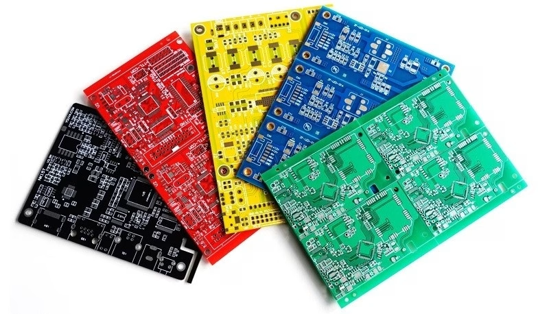
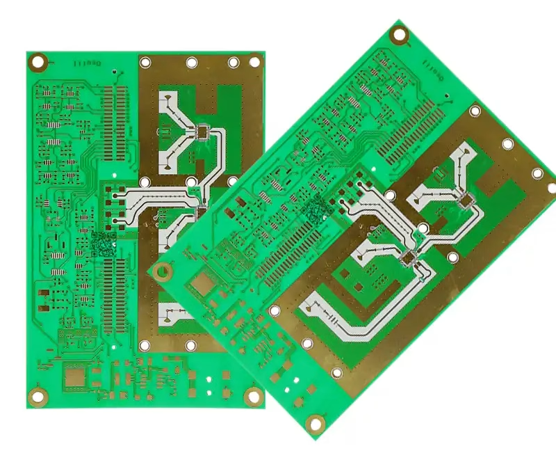
In the rapidly evolving landscape of electronics, the demand for devices operating at higher frequencies continues to escalate. This surge has placed a spotlight on Radio Frequency (RF) and high frequency Printed Circuit Boards (PCBs), which are the foundational components for a vast array of modern technologies. Unlike conventional PCBs, RF PCBs and high frequency circuit boards are engineered to manage signals typically above 500 MHz, often extending into the gigahertz range. This specialized domain demands precision in material selection, design, and manufacturing to ensure optimal signal integrity, minimal loss, and reliable performance.
An RF printed circuit board serves as the backbone for critical applications such as wireless communication systems, radar, satellite technology, and advanced medical equipment. Understanding the intricacies of these boards is crucial for engineers and developers aiming to push the boundaries of high-speed electronic design. This comprehensive guide delves into the specifics of RF and high frequency PCB technology, covering everything from materials and design principles to manufacturing processes and key applications.
2 . The Unique Challenges of RF and High Frequency Circuits
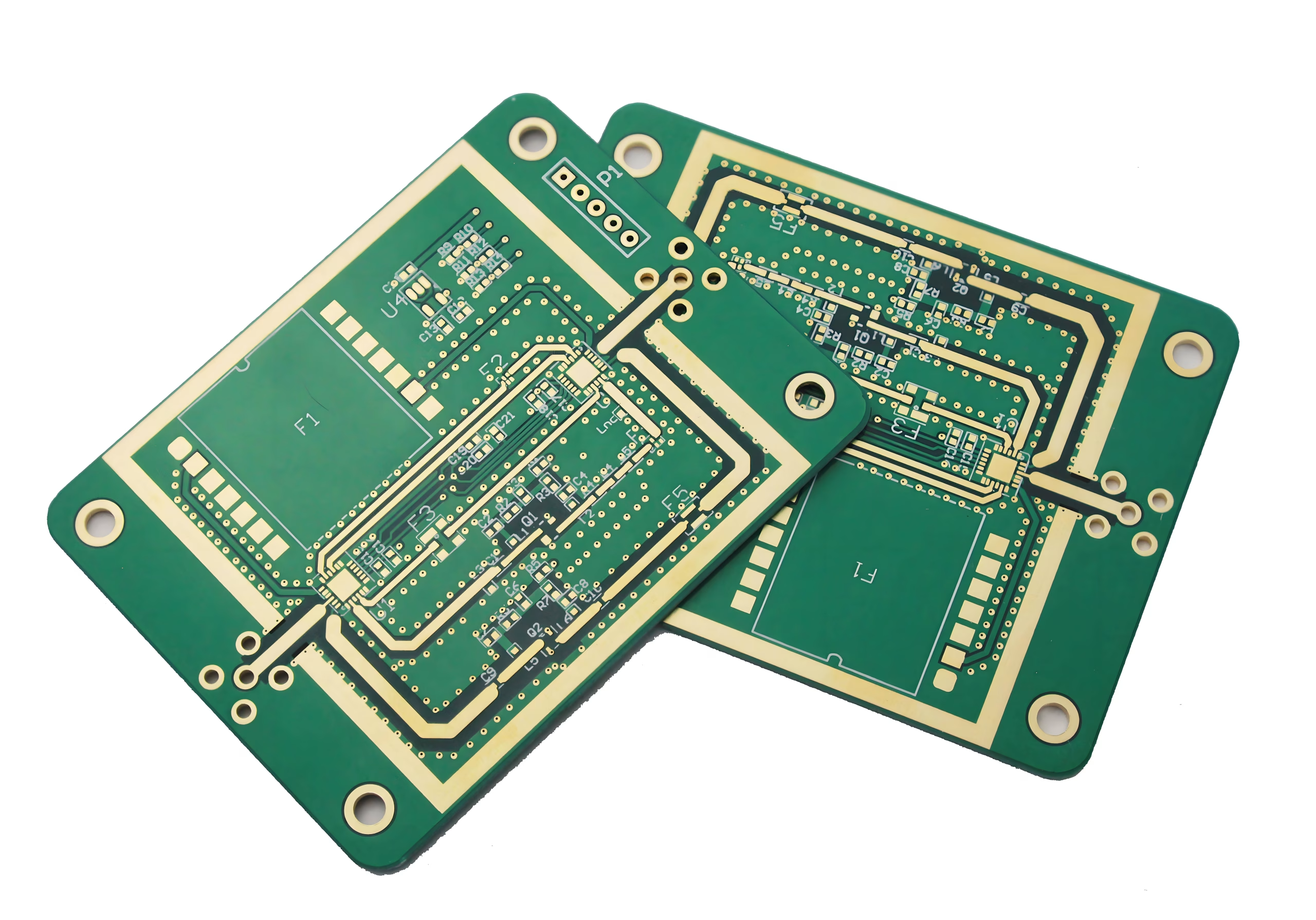
Designing and manufacturing RF circuit boards presents a distinct set of challenges compared to standard digital or low-frequency analog PCBs. At higher frequencies, signals behave less like simple currents and more like electromagnetic waves, making parasitic effects, impedance control, and signal loss significant concerns. Overlooking these factors can lead to signal degradation, system instability, and poor performance.
Key challenges include:
- Signal Integrity:High-frequency signals are highly susceptible to reflections, crosstalk, and electromagnetic interference (EMI). Maintaining signal integrity requires meticulous impedance matching and careful trace routing .
- Dielectric Loss:The PCB substrate itself can absorb signal energy, leading to power loss. This “dissipation factor” becomes critical at higher frequencies.
- Impedance Control:Traces on an RF prototype board must maintain a precise impedance (typically 50 ohms or 75 ohms) to prevent signal reflections. This requires accurate trace width, dielectric thickness, and material consistency.
- Skin Effect:At high frequencies, current tends to flow on the surface of conductors, increasing resistance and trace losses.
- Radiation:Traces can act as antennas, radiating energy and causing EMI if not properly designed and shielded.
- Thermal Management:High frequency components can generate significant heat, requiring effective thermal dissipation strategies.
3. Essential RF and High Frequency PCB Materials
The choice of RF PCB material is arguably the most critical decision in designing a high frequency circuit board. Standard FR-4, while cost -effective for many applications, often exhibits unacceptable performance at frequencies above 1GHz due to its higher dielectric constant (Dk) variability, higher dissipation factor (Df), and poor thermal stability. Specialized materials are essential for high frequency PCB materials.
Key material properties to consider:
- Dielectric Constant (Dk):Also known as relative permittivity. A stable, low Dk is preferred to minimize phase variation with frequency and ensure predictable impedance.
- Dissipation Factor (Df):Also known as loss tangent. Represents the inherent energy loss in the dielectric material. A lower Df is crucial for minimizing signal attenuation, especially at higher frequencies.
- Thermal Stability (Tg and Td):The glass transition temperature (Tg) and decomposition temperature (Td) indicate a material’s resistance to heat. High thermal stability ensures reliability during manufacturing and operation.
- Coefficient of Thermal Expansion (CTE):Mismatch in CTE between the PCB material and components can lead to solder joint stress and component failure.
- Moisture Absorption:High moisture absorption can alter Dk and Df, negatively impacting performance.
Common RF PCB board materials include:
| Material Type | Key Characteristics | Typical Dk (at 10 GHz) | Typical Df (at 10 GHz) | Primary Applications |
| PTFE (Polytetrafluoroethylene) – e.g., Rogers, Taconic | Excellent Dk/Df stability, low loss, wide operating temperature. High cost. | 2.2 to 10.2 | 0.0009 to 0.004 | Radar, satellite, aerospace, advanced telecom |
| Hydrocarbon Ceramics | Good Dk/Df stability, lower cost than pure PTFE, good adhesion. | 3.0 to 10.0 | 0. 0019 to 0.0035 | Automotive radar, base stations, amplifiers |
| Modified FR-4 (High Performance) | Improved D k/Df over standard FR-4, better thermal performance. Cost-effective for mid-range RF. | 3.5 to 4.5 | 0.005 to 0.009 | Wireless LAN, low-cost RF modules |
| Ceramic-filled Thermoset | Blend of properties, good for specific Dk requirements. | 3.0 to 6.0 | 0.002 to 0.005 | Antennas, power amplifiers |
4. Critical Design Considerations for RF PCBs
Effective RF PCB design goes beyond component placement; it involves a holistic approach to layout, routing, and stack-up to mitigate high-frequency challenges. Here are key considerations:
1) Impedance Matching : All transmission lines (traces carrying RF signals) must be impedance controlled, usually to 50 ohms. This involves precise calculation of trace width, dielectric height, and copper thickness.
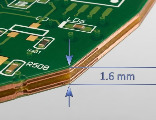
2) Stack-up Design: A well-designed stack-up is crucial for defining impedance, minimizing crosstalk, and providing adequate ground planes. Multiple ground layers and close proximity between signal and ground planes are often employed.
3) Ground Planes: Solid, continuous ground planes are essential for providing a low-impedance return path for RF signals and for shielding sensitive traces. Vias should be strategically placed to stitch ground planes together.
4) Trace Routing:
- Keep Traces Short and Direct:Minimize trace length to reduce loss and radiation.
- Avoid Sharp Corners:Use smooth curves or two 45-degree bends instead of 90-degree corners to prevent impedance discontinuities.
- Maintain Spacing:Adequate spacing between RF traces and other signals (including digital) prevents crosstalk.
- Shielding:Grounded guard traces or shielding enclosures may be necessary for sensitive signals .
5) Via Minimization and Optimization: Vias introduce inductance and capacitance, which can impact impedance. Minimize their use on RF paths, or use “back-drilled” or “blind or buried” vias to reduce stub length.
6) Component Placement: Place RF components close to each other to minimize trace lengths. Keep sensitive RF sections isolated from noisy digital sections.
7) Power Supply Decoupling: Proper decoupling with capacitors placed close to IC power pins is vital to prevent noise propagation.
5. Manufacturing RF and High Frequency PCBs
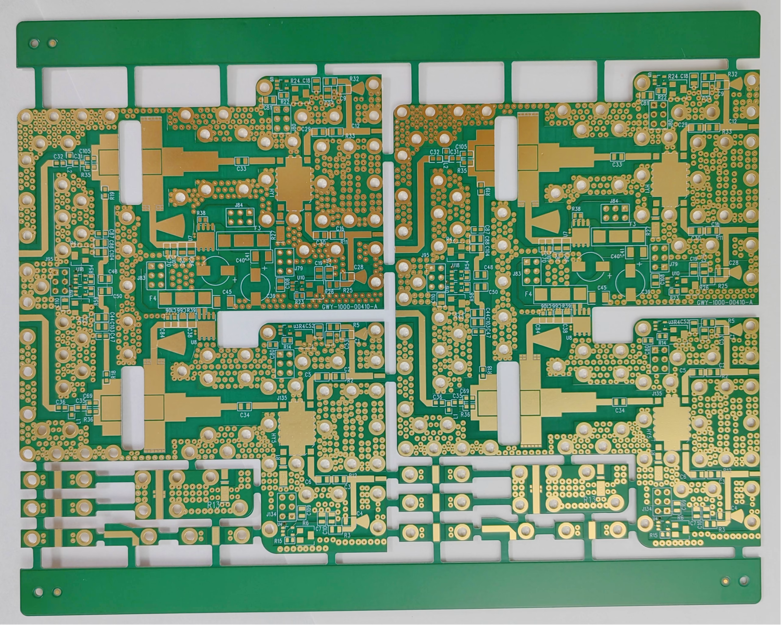
Manufacturing high frequency circuit boards require specialized processes and stringent quality control. The precision demanded by RF designs means that tolerances are much tighter than for standard PCBs. A reputable RF PCB manufacturer or high frequency PCB manufacturer will possess advanced equipment and expertise.
Key manufacturing considerations:
- Material Handling:Specialized RF materials often require specific handling, lamination, and drilling parameters.
- Etching Precision:Achieving tight trace width and spacing tolerances is critical for impedance control. Advanced etching techniques are employed .
- Drilling Accuracy:Precise drilling for vias, especially micro-vias, is essential.
- Lamination Process:The lamination of multiple layers must be carefully controlled to ensure consistent dielectric thickness, which directly impacts impedance.
- Surface Finishes:Selecting the right surface finish (e.g., ENIG, Immersion Silver) is important for solderability and signal integrity at high frequencies.
- Quality Control and Testing:Comprehensive testing, including Time Domain Reflectometry (TDR) for impedance verification and network analysis for S-parameter measurement, is crucial.
6. Key Applications of RF Circuit Boards
The versatility and performance of RF and high frequency PCBs make them indispensable across a wide spectrum of industries. Their ability to handle high-speed signals with minimal loss enables the development of cutting-edge technologies.
Major applications include:
- Telecommunications:5G infrastructure, base stations, cellular phones, Wi-Fi routers, satellite communication systems.
- Aerospace and Defense:Radar systems, electronic warfare, missile guidance, avionics, military radios.
- Automotive:Autonomous driving sensors (LiDAR, radar), infotainment systems, vehicle-to-everything (V2X ) communication.
- Medical Devices:MRI machines, diagnostic equipment, patient monitoring, high-frequency surgical tools.
- Consumer Electronics:Smart home devices, wearable tech, high-speed data transfer , gaming consoles.
- Industrial:RFID systems, industrial automation, IoT devices, high-frequency testing equipment.
7. Choosing an RF PCB Manufacturer
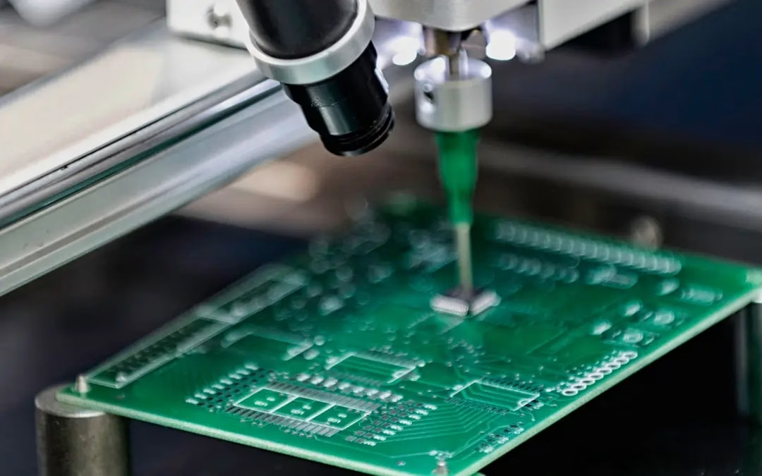
Selecting the right RF PCB manufacturer is paramount for the success of your project. Expertise in high-frequency design and manufacturing is not universal, and working with an inexperienced vendor can lead to costly delays and performance issues.
Factors to consider:
- Experience with RF Materials:Ensure the manufacturer has extensive experience with the specific RF materials you plan to use (e.g., Rogers, Arlon, Isola).
- Advanced Equipment:Look for manufacturers with state-of-the-art equipment for precise etching, drilling, and lamination required for tight tolerances.
- Testing Capabilities:The manufacturer should offer comprehensive testing, including TDR for impedance control, and potentially S-parameter testing.
- Design Support:Some manufacturers offer design rule checking (DRC) and DFM (Design For Manufacturability) services specific to RF boards.
- Certifications:Relevant industry certifications (e.g., ISO, AS9100 for aerospace) can indicate adherence to quality standards.
- Turnaround Time and Cost:Balance lead times with budget, understanding that specialized RF PCBs generally have higher costs due to materials and process complexity.
8. RF PCB and High Frequency PCB FAQs
The primary difference lies in the frequencies they handle. RF PCBs are designed for high-frequency signals (typically above 500MHz), requiring specialized materials with stable dielectric properties, precise impedance control, and meticulous layout techniques to minimize signal loss and interference. Standard PCBs (like those based on FR-4) are generally for lower frequencies or digital signals where these factors are less critical.
At high frequencies, the PCB substrate significantly impacts signal performance. Materials like standard FR-4 have high dielectric losses (Df ) and inconsistent dielectric constants (Dk), leading to signal attenuation and impedance variations. Specialized RF materials offer stable, low Dk and Df, ensuring signal integrity, consistent impedance, and minimal power loss.
While low-cost RF prototype boards might sometimes utilize enhanced FR-4 for lower RF frequencies (e. g., below 1 GHz), standard FR-4 is generally not recommended for true RF or high-frequency applications. Its high Df, variable Dk, and poor thermal stability at higher frequencies will lead to significant signal loss, impedance mismatches, and unreliable performance.
9. Summary
The design and manufacturing of RF and high frequency PCBs represent a specialized discipline critical to the advancement of modern electronics. These boards are the silent enablers of high-speed communication, advanced sensing, and complex data processing across diverse industries. From the initial selection of advanced low-loss dielectric materials to the precise execution of impedance-controlled trace routing and meticulous manufacturing processes, every step requires a deep understanding of high-frequency physics.
By carefully considering factors such as dielectric constant, dissipation factor, thermal management, and precise impedance matching, engineers can overcome the unique challenges posed by RF signals. Partnering with an experienced RF PCB manufacturer is equally vital, ensuring that theoretical designs translate into reliable, high-performing physical boards capable of meeting the stringent demands of today’s cutting-edge applications.
Key Takeaways
- RF and highfrequency PCBs are essential for applications operating above 500 MHz, demanding specialized design and manufacturing.
- Material selection is paramount; low and stable dielectric constant ( Dk) and dissipation factor (Df) are crucial for signal integrity.
- Impedance control, meticulous trace routing, optimized stack-up, and robust ground planes are non-negotiable design principles.
- Manufacturing requires advanced equipment, tight tolerances, and comprehensive testing (e.g., TDR) to ensure performance.
- RF PCBs are foundational to telecommunications, aerospace, automotive, medical, and consumer electronics.
- Choosing an experienced RF PCB manufacturerwith relevant expertise and testing capabilities is critical for project success.
Table of Contents
- 1. Ievads RF un augstajos frekvencēs Frekvences PCB
- 2. RF un augstfrekvences unikālie izaicinājumi Frekvenču shēmas
- 3. Būtiskākie RF un augstie Frekvences PCB materiāli
- 4. RF PCB kritiskie dizaina apsvērumi
- 5. RF un augstas jaudas ražošana Frekvences PCB
- 6. RF shēmu plates galvenie pielietojumi
- 7. RF PCB ražotāja izvēle
- 8. Bieži uzdotie jautājumi par RF PCB un augstfrekvences PCB
- 9. Kopsavilkums
- Atslēgas
Get Your PCB Quote!


