
Rigid PCB 

Contact Us

Contact us for all your PCB, PCBA, and custom service needs!

pcb

Rigid PCBs Built In-House with Factory Direct Service

Rigid PCBs are printed circuit boards built on solid rigid substrate materials like FR4, providing dimensional stability, high strength, and long-term reliability under mechanical and thermal stress.

We provide end-to-end rigid PCB manufacturing using high-precision CNC drilling, multilayer lamination, and fine-line imaging systems. Our process supports single-sided, double-sided, and multilayer rigid circuit boards, all built in compliance with IPC-6012 Class 2/3, ISO 9001, and RoHS standards.

Rigid PCB

Our Rigid PCB Board Capabilities

Our rigid PCB manufacturing capabilities are built to support scalable production across single-sided boards, power-dense multilayers, and precision HDI stack-ups. From trace resolution to copper plating and surface finish control, we deliver production-level consistency across every rigid PCB order.

We build rigid PCBs from 1 to 64 layers using symmetrical and HDI stackups with via-in-pad, staggered build-ups, or buried cores.

Each rigid PCB board is fabricated using rigid FR4 or high Tg substrate materials such as S1000H and IT180.

We maintain interlayer registration within ±25 μm and dielectric thickness tolerance to ±10%, using vacuum lamination with prepreg-based base material calibrated to match copper layer distribution.

These rigid printed circuit boards suit dense multilayer PCBs with high interconnect complexity.

Specification Details
Materials FR4, High TG FR4, Halogen Free Material, CEM-3, Rogers HF Material
Min. Contour Tolerance ±0.04mm
Layer Counts 1–64 Layers
Min. Finished Diameter of PTH Hole 0.08mm
Finished Copper Thickness Up to 1000 μm
Max. Board Thickness / Hole Ratio 40:1
Finished Board Thickness 0.1–12mm
Min. Solder Mask Bridge 3mil (Min. SMT Pad Space 8mil)
Min. Line/Track Width 1.8mil
Min. Legend (Silkscreen) Track Width 4mil
Min. Drilling Slot Size 0.5mm
Surface Treatment Leaded HASL, Lead Free HASL, Immersion Gold, OSP, Immersion Tin, Immersion Silver, etc.
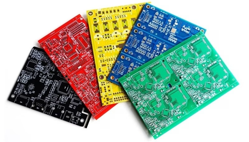
Solder Mask Color Green, Black, Blue, White, Yellow, and Matt, etc.
Legend/Silkscreen Color Black, White, Yellow, and others
Other Technology Gold Finger, Peelable Mask, Non-across Blind/Buried Vias, Characteristic Impedance Control
Solder Mask Hardness 6H
Wrap and Twist ≤0.5%
Flammability 94V-0

We support minimum trace/space widths of 1.8 mil and minimum mechanical drill holes of 0.08 mm with a 4 mil annular ring tolerance.

This allows high-density circuit routing and compact pad arrays for rigid PCBs used in automotive control systems, embedded computing, and advanced power conversion.

Each conductive layer is patterned using LDI and etched with ±10% trace width control. This process enables compact, impedance-sensitive PCB designs across flexible and rigid circuit applications.

We manufacture rigid circuit boards with copper weights ranging from 0.33 to 28 oz per layer, supporting power applications and thermal performance in high-current builds.

Electroplated copper is deposited under 20 to 30 ASF current density and leveled to maintain ±10% thickness uniformity across the panel area.

Conductive layers are verified via cross-section during rigid PCB fabrication to meet Class 3 plating requirements.

We support finished board thicknesses from 0.1 mm to 12 mm, including builds for portable consumer electronics, rigid-flex transition zones, and thick, stiffened boards used in industrial power devices.

Panel thickness uniformity is maintained to ±10%, and bow and twist are controlled under 0.5% post-reflow.

Rigid and flexible stack-ups are supported for hybrid flex PCBs and rigid-flex PCBs with embedded copper planes or stiffeners.

We utilize certified PCB materials, including FR4, halogen-free, and high Tg substrates such as S1000H and IT180, with Tg values ranging from 135 °C to 180 °C and Td values exceeding 340 °C.

These substrate materials allow boards to survive lead-free solder profiles and continuous high-temperature operation.

Each rigid PCB undergoes pre-bake cycles to remove moisture before PCB assembly and reflow.

We provide a full range of surface finishes, including ENIG, OSP, Immersion Silver, Immersion Tin, HASL, and Lead-Free HASL.

All finishes meet RoHS and IPC requirements and are compatible with solder mask layers in high-speed, fine-pitch designs.

Surface treatment is selected based on PCB fabrication goals and printed circuit board performance needs.

Our solder mask layers are applied in green, black, white, blue, red, or yellow using LPI materials with high thermal resistance.

Mask coverage is maintained at 15 to 30 μm thickness over all pads and traces. Single boards or full production panels receive screen-printed epoxy legend in white, black, or yellow, with print resolution up to 150 dpi for text and fiducial marks.

We support V-score panelization, breakaway tabs, routing, and scoring angles from 30° to 60°. Board outline accuracy is controlled to ±0.04 mm with CNC profiling and router bit diameters as small as 0.6 mm.

Each rigid PCB board is panelized to maximize fabrication yield and ensure edge clearance per IPC-2221. These features support WellPCB’s single-sided rigid PCB builds and allow seamless integration with flex tails or overmolded edge connectors.

What Types of Rigid PCBs do we offer?

We offer six rigid PCB types: single-sided, double-sided, multilayer, high Tg, rigid-flex, and metal-backed. Each type is built for a specific function, material requirement, or thermal condition, with defined copper weights, stackups, and supported layer counts.
What is a Rigid PCB?

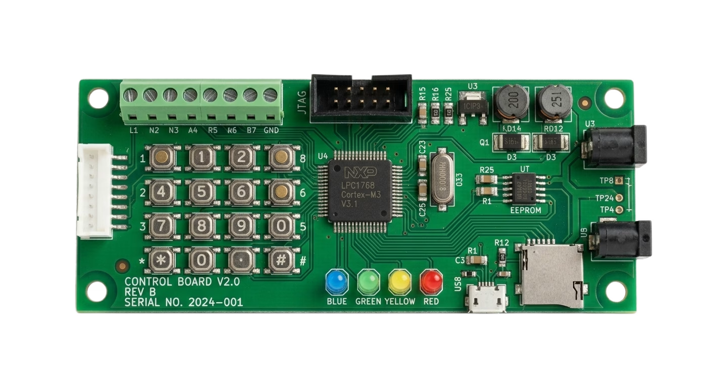
A rigid PCB is a printed circuit board built on a hard, non-bendable substrate, such as rigid FR4, CEM-3, or halogen-free laminate. Each board includes one or more copper layers laminated to the substrate material using heat and adhesive, with finished thicknesses ranging from 0.1 mm to 12 mm.

Standard constructions include single-sided, double-sided, and multilayer PCBs, with stack-ups designed for fixed mounting and dimensional retention. These rigid circuit boards are used when the final assembly requires tight layer registration, consistent pad spacing, and stable circuit performance over time.

What is the Layer Structure of a Rigid PCB?

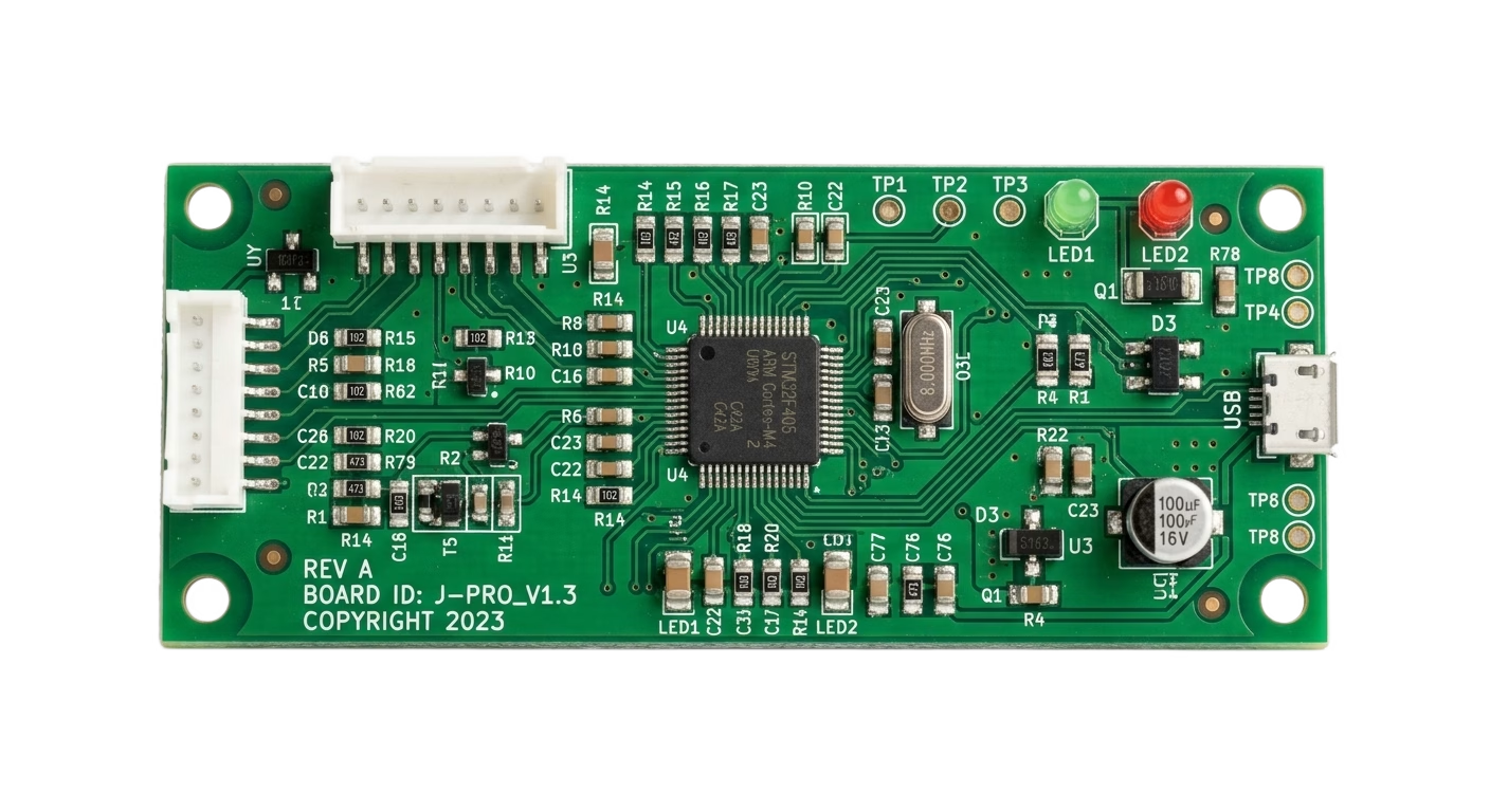
The layer structure of a rigid PCB includes a dielectric substrate, one or more copper layers, a prepreg bonding layer, an outer solder mask, and a printed silkscreen. These layers are compressed into a fixed stack during lamination to form a mechanically rigid and electrically functional board.

Support for PCB Design and Manufacturability

The substrate is the base insulating material that provides the dielectric platform for copper bonding.

Most rigid PCBs use rigid FR4, halogen-free, or high Tg materials with a dielectric constant between 4.2 and 4.6, Tg ≥170 °C, and decomposition temperature over 340 °C.

Depending on the board stack-up, thicknesses range from 0.1 mm to 2.0 mm.

Copper Layer

Solder Mask

Silkscreen is a non-conductive epoxy ink printed on the outer surface for component labeling and assembly reference.

Standard colors include white, yellow, and black. It is applied after the solder mask and must not interfere with exposed copper.

Print resolution typically reaches 0.15 mm line width, allowing precise placement of reference designators and polarity markers.


When Should You Use a Rigid PCB?

Rigid PCBs should be used when the application requires mechanical stability, tight component alignment, or cost-optimized high-volume production. Board selection depends on both product form factor and the specific performance or manufacturing advantages of rigid constructions.

When Product Size and Shape Require Stability

Rigid PCBs are preferred for medium to large-scale electronic devices such as desktop computers, televisions, power amplifiers, and rack-mounted systems.

These assemblies benefit from rigid substrates that maintain flatness, support heavier components, and align with static enclosures.

The non-bendable structure prevents warpage and pad distortion under mechanical load or thermal expansion.

When Application Cost Targets Must Be Met

Rigid boards support predictable, low-cost production by reducing tooling variability and minimizing process adjustments.

Standard FR4 stackups use established lamination flows, simplified layer registration, and repeatable copper foil handling, all of which reduce waste and yield loss in volume runs.

When Shorter Lead Times are Required

Because rigid PCB fabrication uses standardized material sets, stocked copper weights, and stable routing tolerances,it can be completed faster than flexible or hybrid boards.
Most builds ship within 5 to 10 business days, and quick-turn prototypes can be delivered in as little as 48 hours without sacrificing Class 2 or Class 3 process control.

High Component Density

When the design includes dense BGA or QFN placement, rigid PCBs provide pad stability and minimal warpage.

Tighter layout tolerances depend on stable substrate thickness, rigid board thickness control, and reliable solder joint formation across small-pitch components.

Rigid PCB FAQs

Rigid PCBs are built entirely on a solid FR4 or high Tg laminate and remain flat after fabrication. Rigid-flex PCBs combine rigid sections with flexible polyimide layers, allowing dynamic bending or folding during installation.

Rigid boards are ideal for static assemblies with fixed mounting, while rigid-flex designs eliminate connectors between moving parts, reduce weight, and support 3D enclosures.

We support rigid PCB builds down to 0.1 mm finished thickness, using thin-core FR4 and low-flow prepregs for compact or high-density applications. Thickness tolerance is controlled to ±2.5%, with dimensional warpage held under 0.5%.

Yes, we support designs with differential copper thicknesses on inner and outer layers, allowing signal layers to use 0.5 oz while power planes are plated up to 28 oz.

Mixed-weight builds require adjusted lamination pressure and resin flow control to prevent layer distortion.

We maintain dimensional control through balanced stackups, controlled press cycles, and core/prepreg material pairing. For boards larger than 450 × 600 mm, we limit layer count, copper asymmetry, and expansion coefficients to prevent bow and twist beyond 0.5%, as measured post-reflow.

Contact Us

Contact us for all your PCB, PCBA, and custom service needs!

pcb