[email protected]
+86-13570802455
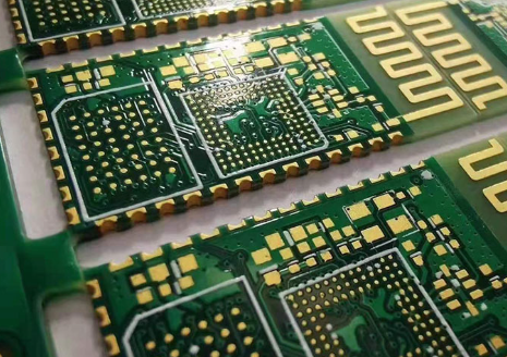
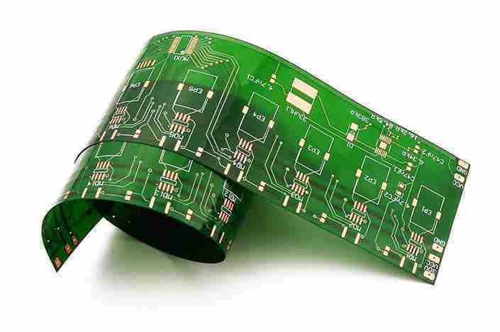
PCBs
Standard PCB prototype pcb HDI PCB High Frequency PCB Halogen-Free PCB High-Tg PCB Flexible PCB Rigid-Flex PCB Double Side PCB SMT Stencil
Applications for PCBs
Automotive PCBs OEM Power Bank PCBs LED PCBs
Materials for PCBs
FR4 PCB Rogers PCB Aluminum PCB Metal Core PCB Heavy Copper PCB Ceramic PCB
Multi Layer PCBs
4 Layer 12 Layer Multilayer PCB
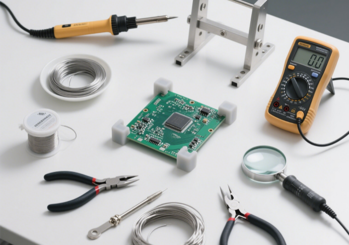
PCBAndAssembly Factory
Assembly Methods
SMT AssemblyTHT PCB AssemblyPOP PackagingAutomated PCB AssemblyCustom PCB AssemblyManual PCB Assembly
PCB Prototype AssemblyQuick Turn PCB AssemblyOne-stop PCB Assembly
Specialized PCB Assemblies
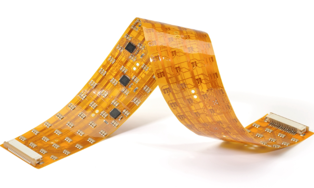
Flexible PCB AssemblyRigid Flex PCB AssemblyAC PCB AssemblyDouble Sided PCB AssemblyCustom PCB AssemblyHigh TG PCB Assembly
Assembly Service Options
Turnkey PCB AssemblyHobbyist PCB Assembly
Production Volume & Cost
PCB Assembly QuoteLow Volume High Mix PCB AssemblyHigh Volume PCB Assembly
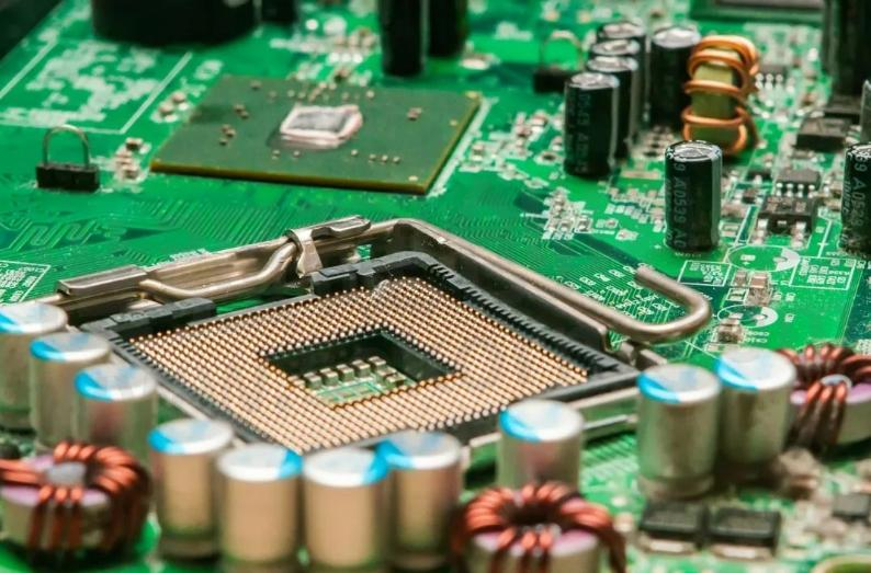
Electronic Components
Manufacturing Capabilities
PCB Manufacturing Capabilities
Quick Turn Available
Quality Control
Automated Optical Inspection (AOI)
Impedance Control
Rapid Prototyping
CNC Machining Services Sheet Metal Fabrication Injection Molding Services 3D Printing Service Electronic Prototype
Technical
Assembly Testing Panel for Assembly BGA Assembly Impedance Control Surface finishing PCB Stack Up PCB Test Advanced Equipment
PCB Design & Resources
PCB Design Impedance Calculator PCB Stack-Up Builder Trace Width Calculator Resistor Color Code Calculator SMD Capacitor Code Calculator SMD Resistor Code Calculator Transmission Line Loss Calculator
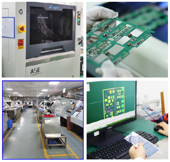
Step into our workshop
Blog
about us
our factory
contact us
FAQ
PCBAndAssembly
We provide PCB, PCB assembly, and Electronic Component Sourcing services.
Continue reading