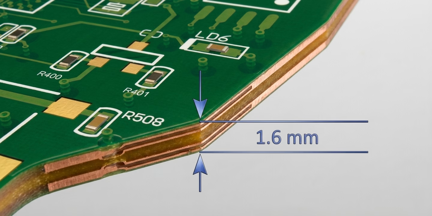
1.6mm PCB: Industry Standards, Thickness, Design Explained
Why is 1.6mm the PCB thickness standard? Get answers on mechanical strength, signal integrity, thermal management, connector compatibility, and when to use alternative thicknesses.
Get Your PCB Quote!
Table of Contents
- 1. Introduction
- 2. Why 1.6mm Became the Global Benchmark
- 3. Anatomy of a 1.6mm PCB: Materials, Layers, and Stackup Configurations
- 4. The Critical Impact of 1.6mm Thickness on Design and Performance
- 5. Beyond 1.6mm: Detailed Comparison with Alternative Thicknesses
- 6. Common Applications for 1.6mm PCB
- 7. When NOT to Use 1.6mm PCB
- 8. Manufacturing and Design Considerations for 1.6mm PCB
- 9. Frequently Asked Questions
- 10. Conclusion
1. Introduction
If you’ve ever worked in electronics design or PCB manufacturing, you’ve undoubtedly encountered the term “1.6mm PCB.” This specific thickness—approximately 0.063 inches or 63 mils—isn’t merely an arbitrary measurement. It represents a deeply embedded industry standard with profound implications for mechanical reliability, electrical performance, connector compatibility, and manufacturing viability. But why is 1.6mm so ubiquitous?
This comprehensive guide illuminates why 1.6mm commands such dominance in the industry, how this thickness ripples through your design and manufacturing decisions, explores practical stackup configurations for various layer counts, and clarifies when alternative thicknesses might better serve your specific project requirements.
2. Why 1.6mm Became the Global Benchmark
The near-universal adoption of 1.6mm PCB thickness didn’t occur by chance. It’s rooted in the fundamental history of printed circuit board manufacturing.
2.1 From Imperial to Metric
The journey of 1.6mm thickness begins during the vacuum tube era, when the electronics industry was in its infancy. Manufacturers required a thickness that could simultaneously provide robust mechanical support for heavy components while remaining economically feasible to produce at scale. The material of choice was phenolic laminate, and through empirical testing, the industry standardized on 1/16 inch as the ideal thickness.
When the global electronics industry transitioned toward metric measurements, a straightforward conversion should have produced 1.5875mm. However, different geographical regions approached the rounding differently. Some standardized on 1.57mm, others on 1.58mm, while the majority settled on 1.6mm. This explains why you may occasionally encounter older specifications citing 1.57mm or the imperial measurement of 62 mils; these all reference the same original 1/16 inch dimension.
| Imperial Origin | Metric Conversion | Common Usage | Industry Prevalence |
| 1/16 inch | 1.5875mm | Rounds to 1.6mm | Most common globally |
| 0.062 inch | 1.5748mm | Often cited as 1.57mm | Seen in some specs |
| 62-63 mils | 1.57-1.60mm | Legacy specifications | Historical references |
| Tolerance range | 1.44-1.76mm | Plus/minus 10% | Manufacturing window |
2.2 Why the Industry Standardized on This Thickness
Multiple converging technical and economic factors cemented 1.6mm as the de facto standard:
Connector Compatibility: One of the most compelling reasons for standardizing on 1.6mm lies in connector design. Throughout the evolution of computer and electronics architecture, board-to-board connectors, edge connectors, and card slots were engineered around the 1/16 inch specification. Deviating from 1.6mm introduces compatibility risks with standard, widely-available connectors.
Manufacturing Economics: Fabricators worldwide invested significantly in optimizing their processes, equipment, and material inventories around the 1.6mm standard. When manufacturers deviate from this standard, they incur process adjustments that incrementally increase manufacturing costs and extend lead times. A non-standard thickness might add 5-15% to unit cost and push delivery dates out by 1-3 days.
Mechanical Balance: Engineering analysis reveals that 1.6mm represents an optimal equilibrium between competing mechanical requirements. The thickness provides sufficient rigidity to support through-hole components and withstand mechanical stresses of assembly and field operation. Yet it remains thin enough to fit into most standard enclosures without imposing weight penalties.
IPC Standardization: Industry standards organizations formalized 1.6mm as the baseline thickness for general-purpose PCBs in foundational standards like IPC-2221. This standardization gave engineers and manufacturers a universally recognized reference point.
3. Anatomy of a 1.6mm PCB: Materials, Layers, and Stackup Configurations
A 1.6mm PCB isn’t monolithic; it’s an intricately engineered stratification of diverse materials, each chosen for specific electrical, thermal, and mechanical properties.
3.1 Materials and Basic Structure
The substrate foundation of nearly all 1.6mm boards is FR4, a glass-reinforced epoxy laminate prized for its exceptional combination of electrical insulation properties, mechanical stability, and cost-effectiveness.
The structure consists of:
- Copper Layers:Typically 35 micrometers thick for outer layers, providing excellent conductivity. Inner layers may be thinner to accommodate more layers within the 1.6mm envelope.
- Dielectric Core:The primary FR4 material, usually 1.0-1.5mm thick, provides mechanical substrate and insulation between copper layers.
- Prepreg (Pre-impregnated):Semi-cured epoxy-glass material that acts as adhesive and insulation in multi-layer boards. Thicknesses typically range from 0.075-0.2mm.
- Solder Mask:A thin polymer layer that protects copper from oxidation and prevents solder bridges during assembly.
- Surface Finish:Protective coating that prevents oxidation and facilitates component soldering.
3.2 Standard 2-Layer 1.6mm PCB Stackup
The simplest and most economical configuration, ideal for low-complexity designs:
| Layer | Material | Thickness | Copper Weight | Purpose |
| Layer 1 (Top) | Copper | 35 microns | 1 oz | Top signal routing |
| Dielectric Core | FR-4 | 1.5mm | — | Mechanical substrate |
| Layer 2 (Bottom) | Copper | 35 microns | 1 oz | Bottom signal routing |
| Total Thickness | — | 1.6mm | — | — |
This stackup suits power supplies, LED drivers, and basic control circuits where electromagnetic compatibility isn’t critical.
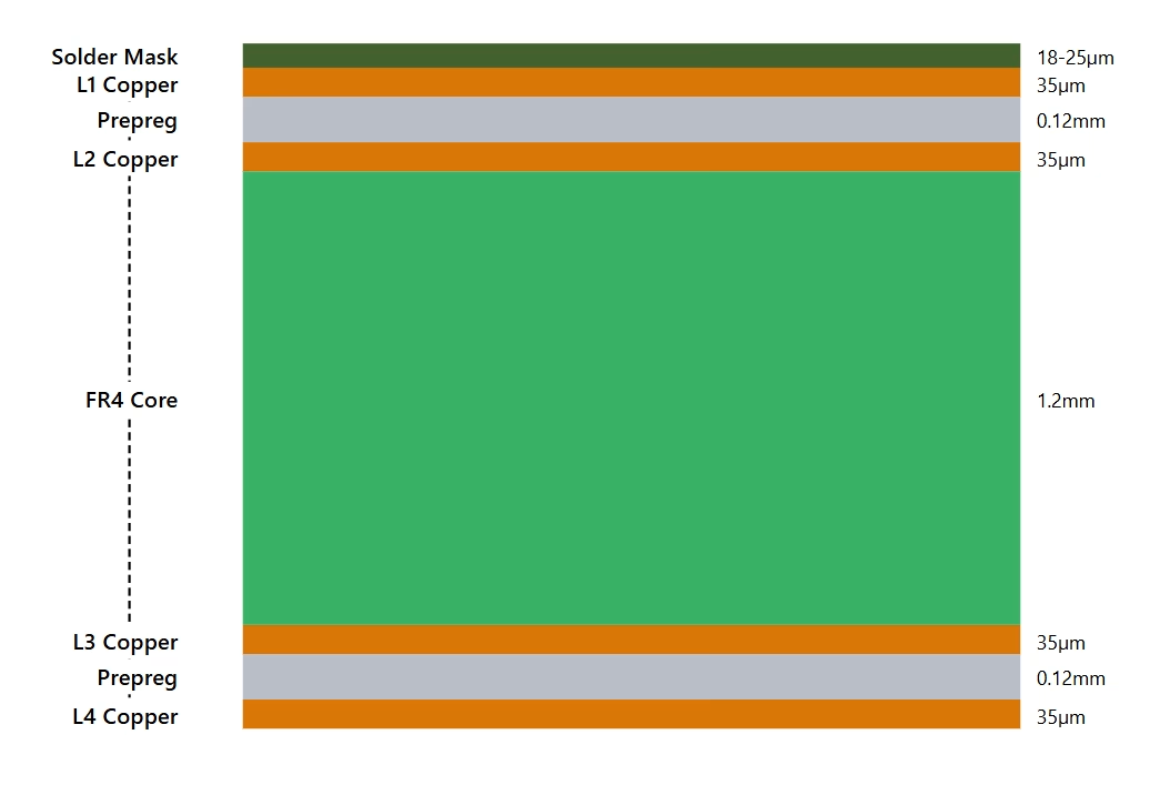
3.3 Standard 4-Layer 1.6mm PCB Stackup
The workhorse configuration for the majority of embedded systems and moderate-complexity designs:
| Layer | Function | Material | Thickness | Copper Weight |
| L1 | Signal | Copper | 35 microns | 1 oz |
| — | Bonding | Prepreg 2116 | 0.12mm | — |
| L2 | Ground Plane | Copper | 35 microns | 1 oz |
| — | Core | FR-4 | 1.2mm | — |
| L3 | Power Plane | Copper | 35 microns | 1 oz |
| — | Bonding | Prepreg 2116 | 0.12mm | — |
| L4 | Signal | Copper | 35 microns | 1 oz |
| Total | — | — | 1.6mm | — |
With dedicated ground and power planes, this configuration delivers excellent electromagnetic immunity and supports impedance-controlled routing on external layers.
3.4 Standard 6-Layer 1.6mm PCB Stackup
Engineered for high-speed digital designs and complex mixed-signal circuits:
| Layer | Function | Material | Thickness | Copper Weight |
| L1 | Signal | Copper | 35 microns | 1 oz |
| — | Bonding | Prepreg 1080 | 0.075mm | — |
| L2 | Ground | Copper | 18 microns | 0.5 oz |
| — | Core | FR-4 | 0.4mm | — |
| L3 | Signal | Copper | 18 microns | 0.5 oz |
| — | Bonding | Prepreg 7628 | 0.2mm | — |
| L4 | Signal | Copper | 18 microns | 0.5 oz |
| — | Core | FR-4 | 0.4mm | — |
| L5 | Power | Copper | 18 microns | 0.5 oz |
| — | Bonding | Prepreg 1080 | 0.075mm | — |
| L6 | Signal | Copper | 35 microns | 1 oz |
| Total | — | — | 1.6mm | — |
The strategic placement of signal layers adjacent to reference planes provides exceptional electromagnetic shielding and enables precise impedance control critical for high-speed applications.
4. The Critical Impact of 1.6mm Thickness on Design and Performance
4.1 Mechanical Strength and Durability
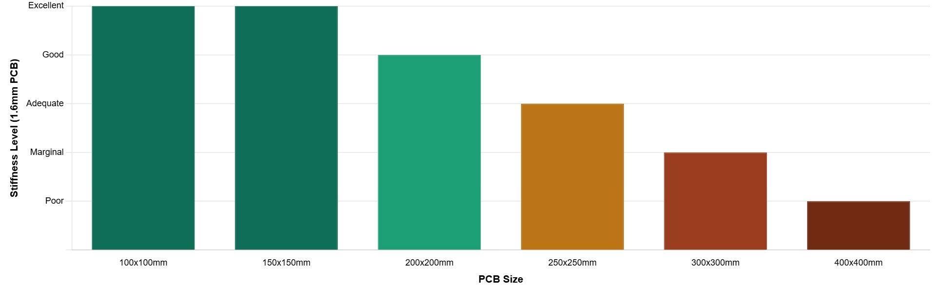
A 1.6mm PCB delivers exceptional mechanical rigidity for boards up to approximately 200mm x 200mm without requiring supplementary stiffeners. The board provides sufficient structural support for heavy discrete components without flexing during assembly or field operation.
| Board Dimensions | 1.6mm Suitability | Recommended Actions |
| Up to 100mm x 100mm | Excellent | No additional support needed |
| 100-200mm | Good | Standard assembly process |
| 200-300mm | Adequate | Monitor for flexing |
| Over 300mm | Marginal | Stiffeners recommended |
4.2 Signal Integrity and Impedance Control
The 1.6mm thickness accommodates well-balanced impedance-controlled stackups. With adequate dielectric spacing between signal and reference planes, designers can reliably achieve controlled impedance traces—typically 50 ohms for single-ended signals or 100 ohms for differential pairs—using practical trace widths.
By contrast, thinner boards compress the available dielectric space, making consistent impedance control problematic and increasing sensitivity to manufacturing variation.
4.3 Thermal Management
Thicker PCBs generally manage thermal dissipation more effectively than thinner alternatives. The additional FR4 material increases thermal mass, allowing the board to absorb and redistribute heat from power-dissipating components.
For designs with moderate power dissipation, 1.6mm provides adequate thermal performance. Designs exceeding 50 watts may benefit from 2.0mm or thicker boards combined with heavy copper techniques.
4.4 Cost Effectiveness
The economic advantage of 1.6mm thickness is substantial. Because it’s the global standard, fabricators maintain optimized processes, material inventories, and equipment configurations specifically for this thickness. Non-standard thicknesses inevitably incur cost premiums and may extend lead times.
| Thickness (mm) | Relative Cost | Lead Time | Notes |
| 0.8mm | +10-20% | +1-2 days | Ultra-compact designs |
| 1.0mm | +5-10% | Standard | Smartphone/wearables |
| 1.2mm | +0-5% | Standard | Portable electronics |
| 1.6mm | Baseline | Fastest (7-10 days) | Industry standard |
| 2.0mm | +10-15% | +1-3 days | Industrial/automotive |
| 2.4mm+ | +20-30% | +3-5 days | Heavy-duty applications |
5. Beyond 1.6mm: Detailed Comparison with Alternative Thicknesses
While 1.6mm dominates, various specialized applications benefit from alternative thicknesses:
| Parameter | 0.8mm | 1.0mm | 1.2mm | 1.6mm | 2.0mm+ |
| Mechanical Strength | Low | Moderate | Good | Excellent | Superior |
| Thermal Dissipation | Limited | Limited | Moderate | Good | Excellent |
| Max Practical Layers | 4 | 6 | 6 | 8+ | 10+ |
| Impedance Control | Difficult | Moderate | Good | Excellent | Excellent |
| Standard Connector Fit | No | Some | Most | Yes | May exceed |
| Relative Cost | +15% | +10% | +5% | Baseline | +10-20% |
| Lead Time Impact | +2 days | +1 day | Standard | Standard | +2-4 days |
Ultra-Thin Options (0.8mm & 1.0mm): Found in smartphones, smartwatches, and IoT modules, they prioritize minimal form factor and weight. However, they sacrifice mechanical strength and complicate impedance control.
Mid-Range Option (1.2mm): A practical compromise between ultra-thin and standard categories, accommodating four-layer stackups while maintaining a relatively compact profile.
Heavy-Duty Options (2.0mm & Above): Deployed in industrial control systems, automotive electronics, and power inverters, they deliver superior mechanical strength and accommodate heavy copper layers for high-current applications.
6. Common Applications for 1.6mm PCB
The versatility of 1.6mm makes it the default choice across diverse industries:
- Computer Motherboards & Expansion Cards:Desktop and embedded computer boards depend on 1.6mm compatibility with standard card slots.
- Industrial Control Systems:PLCs and motor controllers benefit from mechanical robustness and connector standardization.
- Consumer Electronics:Television controllers, home appliances, and audio equipment leverage cost-effectiveness.
- Automotive Electronics:Many ECUs and infotainment systems use 1.6mm boards with high-Tg FR4 materials.
- High-Speed Signal & RF Boards:For RF frequencies up to 5 GHz, standard 1.6mm FR4 serves as an ideal substrate.
- IoT and Embedded Devices:Sensor hubs and gateway devices exploit 1.6mm’s balance of compactness and structural integrity.
7. When NOT to Use 1.6mm PCB
Despite its ubiquity, specific design scenarios benefit from alternative thicknesses:
- Ultra-Compact Mobile Devices:Smartphones and smartwatches may require 0.8mm or 1.0mm boards.
- Credit Card-Sized Devices:Smart cards may mandate 0.4-0.6mm boards.
- High-Power Industrial Equipment:Machinery with large transformers may require 2.0-2.4mm boards.
- Specialized Connector Requirements:Always verify connector specifications before finalizing thickness.
- RF Designs Above 5 GHz:For demanding RF applications, specialized materials with superior dielectric properties become necessary.
8. Manufacturing and Design Considerations for 1.6mm PCB
8.1 Drilling and Via Aspect Ratios
For 1.6mm boards, best practices recommend maintaining minimum hole diameters of 0.25mm for standard fabrication processes. Smaller holes require advanced HDI techniques, increasing cost and lead time.
8.2 Warpage Prevention
Maintain balanced copper distribution between top and bottom layers, and avoid concentrating heavy copper pours on a single side. Symmetrical stackup design is critical for preventing assembly failures.
8.3 Assembly Process Optimization
Standard SMT assembly processes are optimized for 1.6mm boards. Thinner boards may require custom carrier fixtures to prevent warping during reflow, increasing complexity and cost.
8.4 Tolerance Accommodation
Standard thickness tolerance is plus/minus 10%, meaning a nominally 1.6mm board could be 1.44mm to 1.76mm. Design enclosure slots to accommodate this range.
9. Frequently Asked Questions
Q1: Why is 1.6mm the standard PCB thickness?
The 1.6mm standard originated from the imperial measurement of 1/16 inch, which represented the optimal thickness for early phenolic laminate boards. When the industry transitioned to metric measurements, this became 1.5875mm, rounded to 1.6mm. IPC standards subsequently formalized this as the baseline, creating a self-reinforcing standard.
Q2: What is the difference between 1.6mm, 1.57mm, and 62 mil?
They all reference the same original imperial dimension of 1/16 inch. Different regions and eras rounded this differently. For practical purposes, manufacturers treat these as interchangeable.
Q3: Can I fit 6 or 8 layers in a 1.6mm PCB?
Yes. Six-layer boards are straightforward using standard materials. Eight-layer boards fit within 1.6mm but require thinner core materials, making impedance control more sensitive to manufacturing tolerances.
Q4: Is 1.6mm PCB suitable for RF designs?
For moderate RF frequencies up to 3-5 GHz, standard 1.6mm FR4 performs adequately with proper stackup design. For demanding RF applications exceeding 5 GHz, specialized materials with superior dielectric properties become necessary.
Q5: How does 1.6mm thickness affect assembly costs?
Standard SMT assembly equipment accommodates 1.6mm without modification. Maintaining 1.6mm simplifies assembly, reduces fixture requirements, and minimizes risk of warping or defects.
10. Conclusion
The 1.6mm PCB represents a testament to engineering optimization, achieving a near-perfect equilibrium between mechanical strength, material cost, manufacturing efficiency, and connector compatibility. Its dominance reflects decades of iterative refinement and standardization.
PCBAndAssembly is a PCB manufacturing facility with over 14 years of production experience, specializing primarily in standard 1.6mm thick PCBs. We can also provide custom-thickness PCBs ranging from 0.2mm to 10mm, tailored to your specific requirements. If you are seeking a reliable PCB supplier, please send us your Gerber files today; we will provide a complimentary DFM check and quotation for your evaluation.
Table of Contents
- 1. Introduction
- 2. Why 1.6mm Became the Global Benchmark
- 3. Anatomy of a 1.6mm PCB: Materials, Layers, and Stackup Configurations
- 4. The Critical Impact of 1.6mm Thickness on Design and Performance
- 5. Beyond 1.6mm: Detailed Comparison with Alternative Thicknesses
- 6. Common Applications for 1.6mm PCB
- 7. When NOT to Use 1.6mm PCB
- 8. Manufacturing and Design Considerations for 1.6mm PCB
- 9. Frequently Asked Questions
- 10. Conclusion

Get Your PCB Quote!